ZHCSDC3D June 2014 – September 2016 AM4372 , AM4376 , AM4377 , AM4378 , AM4379
PRODUCTION DATA.
- 1器件概述
- 2修订历史记录
- 3Device Comparison
-
4Terminal Configuration and Functions
- 4.1
Pin Diagrams
- ZDN Ball Map [Section Top Left - Top View]
- Table 4-1 ZDN Ball Map [Section Top Middle - Top View]
- Table 4-2 ZDN Ball Map [Section Top Right - Top View]
- Table 4-3 ZDN Ball Map [Section Middle Left - Top View]
- ZDN Ball Map [Section Middle Middle - Top View]
- ZDN Ball Map [Section Middle Right - Top View]
- Table 4-4 ZDN Ball Map [Section Bottom Left - Top View]
- Table 4-5 ZDN Ball Map [Section Bottom Middle - Top View]
- Table 4-6 ZDN Ball Map [Section Bottom Right - Top View]
- 4.2 Pin Attributes
- 4.3
Signal Descriptions
- 4.3.1 ADC Interfaces
- 4.3.2 CAN Interfaces
- 4.3.3 Camera (VPFE) Interfaces
- 4.3.4 Debug Subsystem Interface
- 4.3.5 Display Subsystem (DSS) Interface
- 4.3.6 Ethernet (GEMAC_CPSW) Interfaces
- 4.3.7 External Memory Interfaces
- 4.3.8 General Purpose IOs
- 4.3.9 HDQ Interface
- 4.3.10 I2C Interfaces
- 4.3.11 McASP Interfaces
- 4.3.12 Miscellaneous
- 4.3.13 PRU-ICSS0 Interface
- 4.3.14 PRU-ICSS1 Interface
- 4.3.15 QSPI Interface
- 4.3.16 RTC Subsystem Interface
- 4.3.17 Removable Media Interfaces
- 4.3.18 SPI Interfaces
- 4.3.19 Timer Interfaces
- 4.3.20 UART Interfaces
- 4.3.21 USB Interfaces
- 4.3.22 eCAP Interfaces
- 4.3.23 eHRPWM Interfaces
- 4.3.24 eQEP Interfaces
- 4.1
Pin Diagrams
-
5Specifications
- 5.1 Absolute Maximum Ratings
- 5.2 ESD Ratings
- 5.3 Power-On Hours (POH)
- 5.4 Operating Performance Points
- 5.5 Recommended Operating Conditions
- 5.6 Power Consumption Summary
- 5.7 DC Electrical Characteristics
- 5.8 ADC0: Touch Screen Controller and Analog-to-Digital Subsystem Electrical Parameters
- 5.9 ADC1: Analog-to-Digital Subsystem Electrical Parameters
- 5.10 VPP Specifications for One-Time Programmable (OTP) eFuses
- 5.11 Thermal Resistance Characteristics
- 5.12 External Capacitors
- 5.13
Timing and Switching Characteristics
- 5.13.1 Power Supply Sequencing
- 5.13.2
Clock
- 5.13.2.1 PLLs
- 5.13.2.2 Input Clock Specifications
- 5.13.2.3 Input Clock Requirements
- 5.13.2.4 Output Clock Specifications
- 5.13.2.5 Output Clock Characteristics
- 5.13.3 Timing Parameters and Board Routing Analysis
- 5.13.4 Recommended Clock and Control Signal Transition Behavior
- 5.13.5 Controller Area Network (CAN)
- 5.13.6 DMTimer
- 5.13.7
Ethernet Media Access Controller (EMAC) and Switch
- 5.13.7.1
Ethernet MAC and Switch Electrical Data and Timing
- Table 5-23 Ethernet MAC and Switch Timing Conditions
- 5.13.7.1.1 Ethernet MAC/Switch MDIO Electrical Data and Timing
- 5.13.7.1.2
Ethernet MAC and Switch MII Electrical Data and Timing
- Table 5-27 Timing Requirements for GMII[x]_RXCLK - MII Mode
- Table 5-28 Timing Requirements for GMII[x]_TXCLK - MII Mode
- Table 5-29 Timing Requirements for GMII[x]_RXD[3:0], GMII[x]_RXDV, and GMII[x]_RXER - MII Mode
- Table 5-30 Switching Characteristics for GMII[x]_TXD[3:0], and GMII[x]_TXEN - MII Mode
- 5.13.7.1.3 Ethernet MAC and Switch RMII Electrical Data and Timing
- 5.13.7.1.4
Ethernet MAC and Switch RGMII Electrical Data and Timing
- Table 5-34 Timing Requirements for RGMII[x]_RCLK - RGMII Mode
- Table 5-35 Timing Requirements for RGMII[x]_RD[3:0], and RGMII[x]_RCTL - RGMII Mode
- Table 5-36 Switching Characteristics for RGMII[x]_TCLK - RGMII Mode
- Table 5-37 Switching Characteristics for RGMII[x]_TD[3:0], and RGMII[x]_TCTL - RGMII Mode
- 5.13.7.1
Ethernet MAC and Switch Electrical Data and Timing
- 5.13.8
External Memory Interfaces
- 5.13.8.1 General-Purpose Memory Controller (GPMC)
- 5.13.8.2
Memory Interface
- 5.13.8.2.1
DDR3 and DDR3L Routing Guidelines
- 5.13.8.2.1.1 Board Designs
- 5.13.8.2.1.2 DDR3 Device Combinations
- 5.13.8.2.1.3
DDR3 Interface
- 5.13.8.2.1.3.1 DDR3 Interface Schematic
- 5.13.8.2.1.3.2 Compatible JEDEC DDR3 Devices
- 5.13.8.2.1.3.3 DDR3 PCB Stackup
- 5.13.8.2.1.3.4 DDR3 Placement
- 5.13.8.2.1.3.5 DDR3 Keepout Region
- 5.13.8.2.1.3.6 DDR3 Bulk Bypass Capacitors
- 5.13.8.2.1.3.7 DDR3 High-Speed Bypass Capacitors
- 5.13.8.2.1.3.8 DDR3 Net Classes
- 5.13.8.2.1.3.9 DDR3 Signal Termination
- 5.13.8.2.1.3.10 DDR3 DDR_VREF Routing
- 5.13.8.2.1.3.11 DDR3 VTT
- 5.13.8.2.1.4 DDR3 CK and ADDR_CTRL Topologies and Routing Definition
- 5.13.8.2.1.5 Data Topologies and Routing Definition
- 5.13.8.2.1.6 Routing Specification
- 5.13.8.2.2
LPDDR2 Routing Guidelines
- 5.13.8.2.2.1 LPDDR2 Board Designs
- 5.13.8.2.2.2 LPDDR2 Device Configurations
- 5.13.8.2.2.3
LPDDR2 Interface
- 5.13.8.2.2.3.1 LPDDR2 Interface Schematic
- 5.13.8.2.2.3.2 Compatible JEDEC LPDDR2 Devices
- 5.13.8.2.2.3.3 LPDDR2 PCB Stackup
- 5.13.8.2.2.3.4 LPDDR2 Placement
- 5.13.8.2.2.3.5 LPDDR2 Keepout Region
- 5.13.8.2.2.3.6 LPDDR2 Net Classes
- 5.13.8.2.2.3.7 LPDDR2 Signal Termination
- 5.13.8.2.2.3.8 LPDDR2 DDR_VREF Routing
- 5.13.8.2.2.4 Routing Specification
- 5.13.8.2.1
DDR3 and DDR3L Routing Guidelines
- 5.13.9 Display Subsystem (DSS)
- 5.13.10 Camera (VPFE)
- 5.13.11 Inter-Integrated Circuit (I2C)
- 5.13.12 Multichannel Audio Serial Port (McASP)
- 5.13.13 Multichannel Serial Port Interface (McSPI)
- 5.13.14 Quad Serial Port Interface (QSPI)
- 5.13.15 HDQ/1-Wire Interface (HDQ/1-Wire)
- 5.13.16
Programmable Real-Time Unit Subsystem and Industrial Communication Subsystem (PRU-ICSS)
- 5.13.16.1
Programmable Real-Time Unit (PRU-ICSS PRU)
- Table 5-100 PRU-ICSS PRU Timing Conditions
- 5.13.16.1.1 PRU-ICSS PRU Direct Input/Output Mode Electrical Data and Timing
- 5.13.16.1.2 PRU-ICSS PRU Parallel Capture Mode Electrical Data and Timing
- 5.13.16.1.3 PRU-ICSS PRU Shift Mode Electrical Data and Timing
- 5.13.16.1.4 PRU-ICSS Sigma Delta Electrical Data and Timing
- 5.13.16.1.5 PRU-ICSS ENDAT Electrical Data and Timing
- 5.13.16.2
PRU-ICSS EtherCAT (PRU-ICSS ECAT)
- Table 5-109 PRU-ICSS ECAT Timing Conditions
- 5.13.16.2.1
PRU-ICSS ECAT Electrical Data and Timing
- Table 5-110 PRU-ICSS ECAT Timing Requirements - Input Validated With LATCH_IN
- Table 5-111 PRU-ICSS ECAT Timing Requirements - Input Validated With SYNCx
- Table 5-112 PRU-ICSS ECAT Timing Requirements - Input Validated With Start of Frame (SOF)
- Table 5-113 PRU-ICSS ECAT Timing Requirements - LATCHx_IN
- Table 5-114 PRU-ICSS ECAT Switching Requirements - Digital IOs
- 5.13.16.3 PRU-ICSS MII_RT and Switch
- 5.13.16.4 PRU-ICSS Universal Asynchronous Receiver Transmitter (PRU-ICSS UART)
- 5.13.16.1
Programmable Real-Time Unit (PRU-ICSS PRU)
- 5.13.17
Multimedia Card (MMC) Interface
- 5.13.17.1
MMC Electrical Data and Timing
- Table 5-125 MMC Timing Conditions
- Table 5-126 Timing Requirements for MMC[0]_CMD and MMC[0]_DAT[7:0]
- Table 5-127 Timing Requirements for MMC[1/2]_CMD and MMC[1/2]_DAT[7:0]
- Table 5-128 Switching Characteristics for MMC[x]_CLK
- Table 5-129 Switching Characteristics for MMC[x]_CMD and MMC[x]_DAT[7:0]—HSPE=0
- Table 5-130 Switching Characteristics for MMC[x]_CMD and MMC[x]_DAT[7:0]—HSPE=1
- 5.13.17.1
MMC Electrical Data and Timing
- 5.13.18 Universal Asynchronous Receiver/Transmitter (UART)
- 5.14 Emulation and Debug
- 6Device and Documentation Support
- 7Mechanical, Packaging, and Orderable Information
5.13.8.2.1.3.1 DDR3 Interface Schematic
The DDR3 interface schematic varies, depending upon the width of the DDR3 devices used.
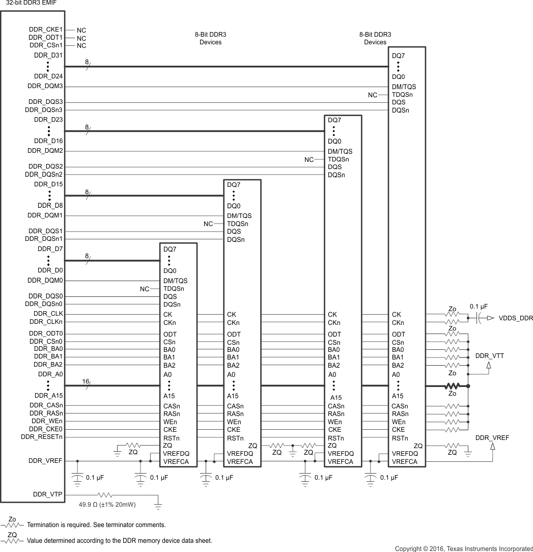
Figure 5-49 shows the schematic connections for 16-bit interface using one x16 DDR3 device. Figure 5-50 shows the schematic connections for 16-bit interface without using VTT termination for the ADDR_CTRL net class signals. Figure 5-51 shows the schematic connections for 16-bit interface using two x8 DDR3 devices.
Figure 5-52 shows the schematic connections for 32-bit interface using two x16 DDR3 device and Figure 5-53 shows the schematic connections for 32-bit interface using four x8 DDR3 devices.
When not using all or part of a DDR3 interface, the proper method of handling the unused pins is to tie off the DDR_DQS[x] pins to the VDDS_DDR supply via a 1-kΩ resistor and pulling the DDR_DQSn[x] pins to ground via a 1k-Ω resistor. This must be done for each byte not used. Although these signals have internal pullup and pulldown, external pullup and pulldown provide additional protection against external electrical noise causing activity on the signals. Also, include the 49.9-Ω pulldown for DDR_VTP. The VDDS_DDR and DDR_VREF power supply terminals need to be connected to their respective power supplies even if the DDR3 interface is not being used. All other DDR3 interface pins can be left unconnected. The supported modes for use of the DDR3 EMIF are 32 bits wide, 16 bits wide, or not used.
The device can only source one load connected to the DQS[x] and DQ[x] net class signals and up to four loads connected to the CK and ADDR_CTRL net class signals. For more information related to net classes, see Section 5.13.8.2.1.3.8.
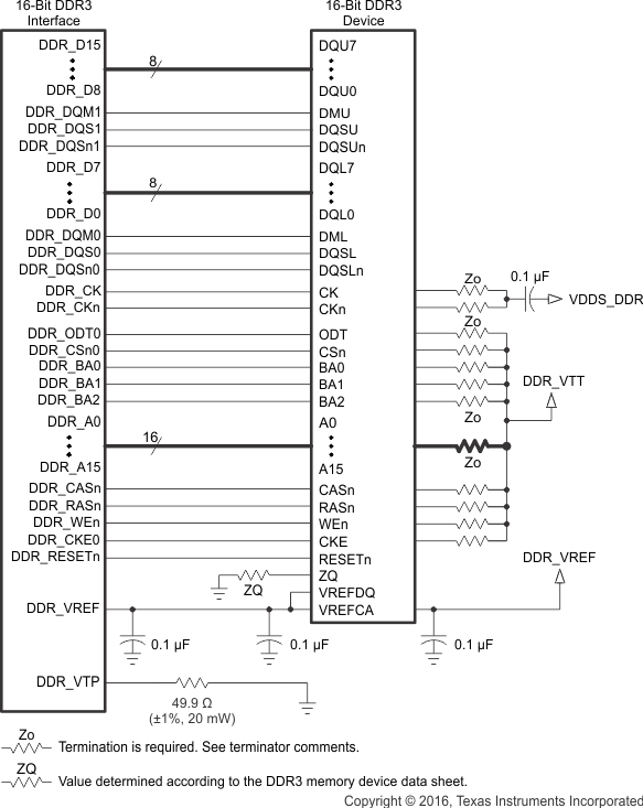 Figure 5-49 16-Bit DDR3 Interface Using One 16-Bit DDR3 Device With VTT Termination
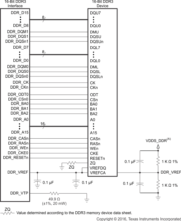
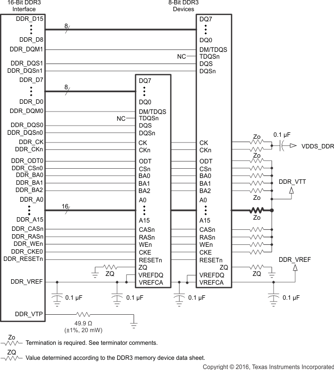 Figure 5-51 16-Bit DDR3 Interface Using Two 8-Bit DDR3 Devices With VTT Termination
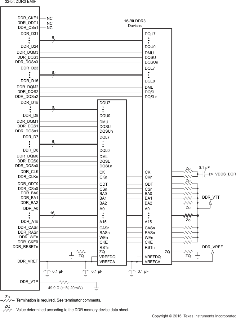 Figure 5-52 32-Bit DDR3 Interface Using Two 16-Bit DDR3 Devices With VTT Termination
