ZHCSH00F August 2016 – November 2019 AM5706 , AM5708
PRODUCTION DATA.
- 1器件概述
- 2修订历史记录
- 3Device Comparison
-
4Terminal Configuration and Functions
- 4.1 Pin Diagram
- 4.2 Pin Attributes
- 4.3
Signal Descriptions
- 4.3.1 VIP
- 4.3.2 DSS
- 4.3.3 HDMI
- 4.3.4 CSI2
- 4.3.5 EMIF
- 4.3.6 GPMC
- 4.3.7 Timers
- 4.3.8 I2C
- 4.3.9 HDQ1W
- 4.3.10 UART
- 4.3.11 McSPI
- 4.3.12 QSPI
- 4.3.13 McASP
- 4.3.14 USB
- 4.3.15 PCIe
- 4.3.16 DCAN
- 4.3.17 GMAC_SW
- 4.3.18 MLB
- 4.3.19 eMMC/SD/SDIO
- 4.3.20 GPIO
- 4.3.21 KBD
- 4.3.22 PWM
- 4.3.23 PRU-ICSS
- 4.3.24 Emulation and Debug Subsystem
- 4.3.25 System and Miscellaneous
- 4.3.26 Power Supplies
- 4.4 Pin Multiplexing
- 4.5 Connections for Unused Pins
-
5Specifications
- 5.1 Absolute Maximum Ratings
- 5.2 ESD Ratings
- 5.3 Power on Hours (POH) Limits
- 5.4 Recommended Operating Conditions
- 5.5 Operating Performance Points
- 5.6 Power Consumption Summary
- 5.7
Electrical Characteristics
- Table 5-7 LVCMOS DDR DC Electrical Characteristics
- Table 5-8 Dual Voltage LVCMOS I2C DC Electrical Characteristics
- Table 5-9 IQ1833 Buffers DC Electrical Characteristics
- Table 5-10 IHHV1833 Buffers DC Electrical Characteristics
- Table 5-11 LVCMOS CSI2 DC Electrical Characteristics
- Table 5-12 BMLB18 Buffers DC Electrical Characteristics
- Table 5-13 Dual Voltage SDIO1833 DC Electrical Characteristics
- Table 5-14 Dual Voltage LVCMOS DC Electrical Characteristics
- 5.7.1 USBPHY DC Electrical Characteristics
- 5.7.2 HDMIPHY DC Electrical Characteristics
- 5.7.3 PCIEPHY DC Electrical Characteristics
- 5.8 VPP Specifications for One-Time Programmable (OTP) eFuses
- 5.9 Thermal Resistance Characteristics for CBD Package
- 5.10
Timing Requirements and Switching Characteristics
- 5.10.1 Timing Parameters and Information
- 5.10.2 Interface Clock Specifications
- 5.10.3 Power Supply Sequences
- 5.10.4 Clock Specifications
- 5.10.5 Recommended Clock and Control Signal Transition Behavior
- 5.10.6
Peripherals
- 5.10.6.1 Timing Test Conditions
- 5.10.6.2 Virtual and Manual I/O Timing Modes
- 5.10.6.3 VIP
- 5.10.6.4 DSS
- 5.10.6.5 HDMI
- 5.10.6.6 CSI2
- 5.10.6.7 EMIF
- 5.10.6.8 GPMC
- 5.10.6.9 Timers
- 5.10.6.10 I2C
- 5.10.6.11 HDQ1W
- 5.10.6.12 UART
- 5.10.6.13 McSPI
- 5.10.6.14 QSPI
- 5.10.6.15 McASP
- 5.10.6.16 USB
- 5.10.6.17 PCIe
- 5.10.6.18 DCAN
- 5.10.6.19
GMAC_SW
- 5.10.6.19.1
GMAC MII Timings
- Table 5-91 Timing Requirements for miin_rxclk - MII Operation
- Table 5-92 Timing Requirements for miin_txclk - MII Operation
- Table 5-93 Timing Requirements for GMAC MIIn Receive 10/100 Mbit/s
- Table 5-94 Switching Characteristics Over Recommended Operating Conditions for GMAC MIIn Transmit 10/100 Mbits/s
- 5.10.6.19.2 GMAC MDIO Interface Timings
- 5.10.6.19.3
GMAC RMII Timings
- Table 5-99 Timing Requirements for GMAC REF_CLK - RMII Operation
- Table 5-100 Timing Requirements for GMAC RMIIn Receive
- Table 5-101 Switching Characteristics Over Recommended Operating Conditions for GMAC REF_CLK - RMII Operation
- Table 5-102 Switching Characteristics Over Recommended Operating Conditions for GMAC RMIIn Transmit 10/100 Mbits/s
- 5.10.6.19.4
GMAC RGMII Timings
- Table 5-106 Timing Requirements for rgmiin_rxc - RGMIIn Operation
- Table 5-107 Timing Requirements for GMAC RGMIIn Input Receive for 10/100/1000 Mbps
- Table 5-108 Switching Characteristics Over Recommended Operating Conditions for rgmiin_txctl - RGMIIn Operation for 10/100/1000 Mbit/s
- Table 5-109 Switching Characteristics for GMAC RGMIIn Output Transmit for 10/100/1000 Mbps
- 5.10.6.19.1
GMAC MII Timings
- 5.10.6.20
eMMC/SD/SDIO
- 5.10.6.20.1
MMC1—SD Card Interface
- 5.10.6.20.1.1 Default speed, 4-bit data, SDR, half-cycle
- 5.10.6.20.1.2 High speed, 4-bit data, SDR, half-cycle
- 5.10.6.20.1.3 SDR12, 4-bit data, half-cycle
- 5.10.6.20.1.4 SDR25, 4-bit data, half-cycle
- 5.10.6.20.1.5 UHS-I SDR50, 4-bit data, half-cycle
- 5.10.6.20.1.6 UHS-I SDR104, 4-bit data, half-cycle
- 5.10.6.20.1.7 UHS-I DDR50, 4-bit data
- 5.10.6.20.2 MMC2 — eMMC
- 5.10.6.20.3 MMC3 and MMC4—SDIO/SD
- 5.10.6.20.1
MMC1—SD Card Interface
- 5.10.6.21 GPIO
- 5.10.6.22
PRU-ICSS
- 5.10.6.22.1 Programmable Real-Time Unit (PRU-ICSS PRU)
- 5.10.6.22.2
PRU-ICSS EtherCAT (PRU-ICSS ECAT)
- 5.10.6.22.2.1
PRU-ICSS ECAT Electrical Data and Timing
- Table 5-164 PRU-ICSS ECAT Timing Requirements – Input Validated With LATCH_IN
- Table 5-165 PRU-ICSS ECAT Timing Requirements – Input Validated With SYNCx
- Table 5-166 PRU-ICSS ECAT Timing Requirements – Input Validated With Start of Frame (SOF)
- Table 5-167 PRU-ICSS ECAT Timing Requirements - LATCHx_IN
- Table 5-168 PRU-ICSS ECAT Switching Requirements - Digital IOs
- 5.10.6.22.2.1
PRU-ICSS ECAT Electrical Data and Timing
- 5.10.6.22.3 PRU-ICSS MII_RT and Switch
- 5.10.6.22.4 PRU-ICSS Universal Asynchronous Receiver Transmitter (PRU-ICSS UART)
- 5.10.6.22.5 PRU-ICSS IOSETs
- 5.10.6.22.6 PRU-ICSS Manual Functional Mapping
- 5.10.6.23 System and Miscellaneous interfaces
- 5.10.7
Emulation and Debug Subsystem
- 5.10.7.1
IEEE 1149.1 Standard-Test-Access Port (JTAG)
- 5.10.7.1.1
JTAG Electrical Data/Timing
- Table 5-194 Timing Requirements for IEEE 1149.1 JTAG
- Table 5-195 Switching Characteristics Over Recommended Operating Conditions for IEEE 1149.1 JTAG
- Table 5-196 Timing Requirements for IEEE 1149.1 JTAG With RTCK
- Table 5-197 Switching Characteristics Over Recommended Operating Conditions for IEEE 1149.1 JTAG With RTCK
- 5.10.7.1.1
JTAG Electrical Data/Timing
- 5.10.7.2 Trace Port Interface Unit (TPIU)
- 5.10.7.1
IEEE 1149.1 Standard-Test-Access Port (JTAG)
-
6Detailed Description
- 6.1 Description
- 6.2 Functional Block Diagram
- 6.3 MPU
- 6.4 DSP Subsystem
- 6.5 PRU-ICSS
- 6.6 Memory Subsystem
- 6.7 Interprocessor Communication
- 6.8 Interrupt Controller
- 6.9 EDMA
- 6.10 Peripherals
- 6.11 On-chip Debug
-
7Applications, Implementation, and Layout
- 7.1 Power Supply Mapping
- 7.2
DDR3 Board Design and Layout Guidelines
- 7.2.1 DDR3 General Board Layout Guidelines
- 7.2.2
DDR3 Board Design and Layout Guidelines
- 7.2.2.1 Board Designs
- 7.2.2.2 DDR3 EMIF
- 7.2.2.3 DDR3 Device Combinations
- 7.2.2.4 DDR3 Interface Schematic
- 7.2.2.5 Compatible JEDEC DDR3 Devices
- 7.2.2.6 PCB Stackup
- 7.2.2.7 Placement
- 7.2.2.8 DDR3 Keepout Region
- 7.2.2.9 Bulk Bypass Capacitors
- 7.2.2.10 High-Speed Bypass Capacitors
- 7.2.2.11 Net Classes
- 7.2.2.12 DDR3 Signal Termination
- 7.2.2.13 VREF_DDR Routing
- 7.2.2.14 VTT
- 7.2.2.15 CK and ADDR_CTRL Topologies and Routing Definition
- 7.2.2.16 Data Topologies and Routing Definition
- 7.2.2.17 Routing Specification
- 7.3 High Speed Differential Signal Routing Guidance
- 7.4 Power Distribution Network Implementation Guidance
- 7.5 Thermal Solution Guidance
- 7.6 Single-Ended Interfaces
- 7.7 LJCB_REFN/P Connections
- 7.8 Clock Routing Guidelines
- 8Device and Documentation Support
- 9Mechanical, Packaging, and Orderable Information
5.10.3 Power Supply Sequences
This section describes the power-up and power-down sequence required to ensure proper device operation. The power supply names described in this section comprise a superset of a family of compatible devices. Some members of this family will not include a subset of these power supplies and their associated device modules. Refer to the Section 4.2, Pin Attributes of the Section 4, Terminal Configuration and Functions to determine which power supplies are applicable.
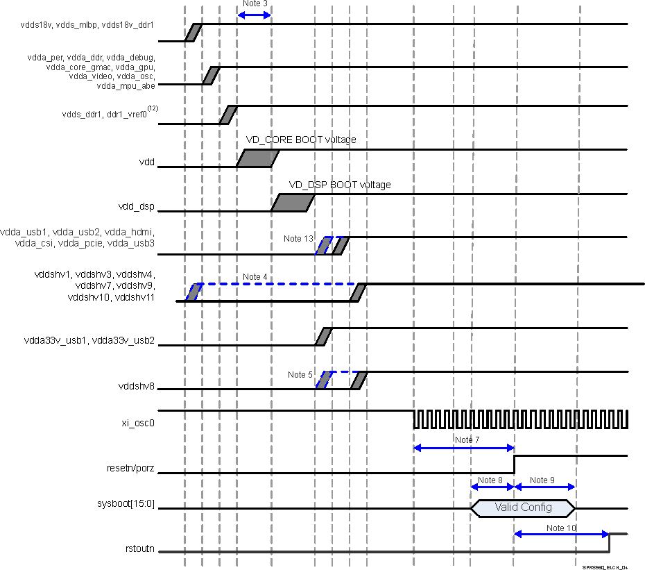
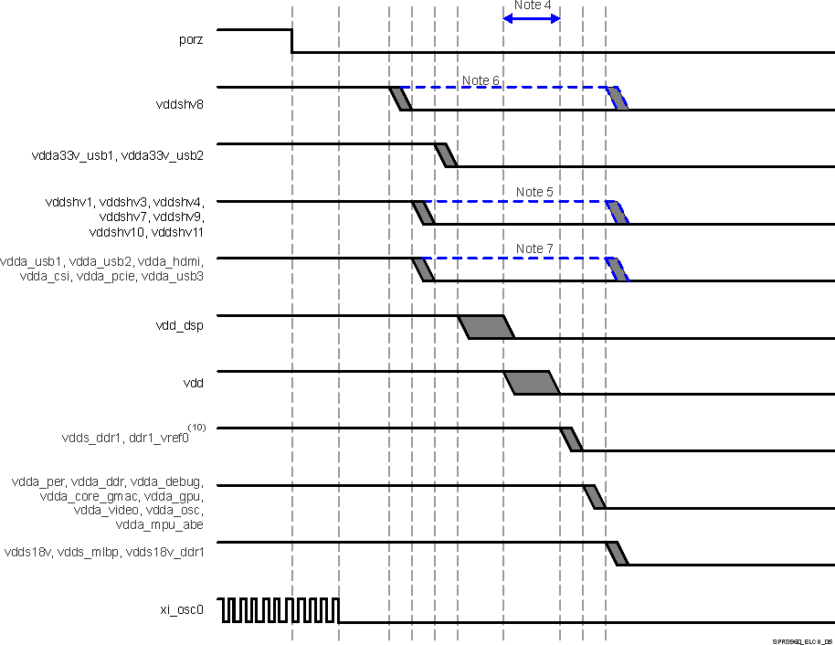
Figure 5-5 and Figure 5-6, describe the device Power Sequencing.
 Figure 5-5 Power-Up Sequencing
 - Grey shaded areas are windows where it is valid to ramp the voltage rail.
- Blue dashed lines are not valid windows but show alternate ramp possibilities based on the associated note.
- vdd must ramp before or at the same time as vdd_dsp.
- If any of the vddshv1, vddshv3, vddshv4, vddshv7, vddshv[9-11] rails (not including vddshv8) are used as 1.8V only, then these rails can be combined with vdds18v.
- vddshv8 is separated out to show support for dual voltage. If single voltage is used then vddshv8 can be combined with other vddshvn rails but vddshv8 must ramp after vdd.
- vdds and vdda rails must not be combined together.
- porz must remain asserted low until all of the following conditions are met:
- All device supply rails reach stable operational levels.
- xi_osc0 is stable and at a valid frequency.
- Minimum of 12P after both of the above conditions are met, where P = 1 / (SYS_CLK1/610), units in ns.
resetn must be high prior to, or rise simultaneous with, porz but not before its power supply, vddshv3, rising.
- Setup time: sysboot[15:0] pins must be valid 2P(11) before porz is de-asserted high.
- Hold time: sysboot[15:0] pins must be valid 15P(11) after porz is de-asserted high.
- rstoutn will be asserted low when porz is low, and de-asserted following an internal 2ms delay. rstoutn is only valid after vddshv3 reaches an operational level. If used as a peripheral component reset, it should be AND gated with porz to avoid possible reset glitches during power up.
- P = 1/(SYS_CLK1/610) frequency in ns.
- ddr1_vref0 may rise coincident with vdds_ddr1 or at a later time. However, it must be valid before porz rising.
- vdda_usb1, vdda_usb2, vdda_hdmi, vdda_pcie, vdda_usb3 can be energized concurrently or after vdda33v_usb1, vdda33v_usb2.
- Grey shaded areas are windows where it is valid to ramp the voltage rail.
- Blue dashed lines are not valid windows but show alternate ramp possibilities based on the associated note.
- xi_osc0 can be turned off anytime after porz assertion and must be turned off before vdda_osc voltage rail is shutdown.
- vdd must ramp after or at the same time as vdd_dsp.
- If any of the vddshv1, vddshv3, vddshv4, vddshv7, vddshv[9-11] rails (not including vddshv8) are used as 1.8V only, then these rails can be combined with vdds18v.
- vddshv1, vddshv3, vddshv4, vddshv7, vddshv[9-11] is allowed to ramp down at either of the two points shown in the timing diagram in either 1.8V mode or in 3.3V mode.
- If vddshv1, vddshv3, vddshv4, vddshv7, vddshv[9-11] ramps down at the later time in the diagram then the board design must ensure that the vddshv[1, 3-4, 7, 9-11] rail is never higher than 2.0 V above the vdds18v rail.
- vddshv8 is separated out to show support for dual voltage. If a dedicated LDO/supply source is used for vddshv8, then vddshv8 ramp down should occur at one of the two earliest points in the timing diagram. If vddshv8 is powered by the same supply source as the other vddshvn rails, then it is allowed to ramp down at either of the last two points in the timing diagram.
- The 1.8V vdda_* supplies can either ramp down at the earlier time period shown or can be delayed to ramp down after the core supplies coincident with the vdds18v supply as long as porz is asserted (low) during the power down sequence.
- The power down sequence shown is the most general case and is always valid. An accelerated power down sequence is also available but is only valid when porz is asserted (low). This accelerated power down sequence has been implemented in the companion PMIC that is recommended for use with this SoC. The accelerated sequence has porz go low first followed immediately by 3.3V vddshvx supplies and vddshv8 simultaneously second, 1.8V PHY, 3.3V USB and core supplies simultaneously third, DDR supplies, DDR references and 1.8V PLL supplies simultaneously fourth and all other 1.8V supplies simultaneously last.
- Ramped Down is defined as reaching a voltage level of no more than 0.6V.
- ddr1_vref0 may fall coincident with vdds_ddr1, or at a prior time but after porz is asserted low.
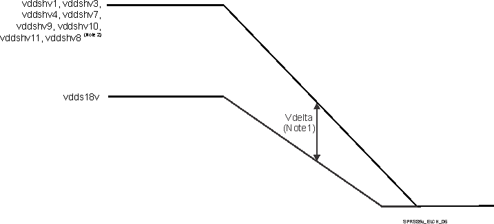
Figure 5-7 describes vddshv[1, 3-4, 7, 9-11] Supplies Falling Before vdds18v Supplies Delta.
 Figure 5-7 vddshv* Supplies Falling After vdds18v Supplies Delta
 - Vdelta MAX = 2V
- If vddshv8 is powered by the same supply source as the other vddshv[1, 3-4, 7, 9-11] rails.
