ZHCSF38G March 2016 – May 2018 AM5716 , AM5718
PRODUCTION DATA.
- 1 器件概述
- 2 修订历史记录
- 3 Device Comparison
-
4 Terminal Configuration and Functions
- 4.1 Terminal Assignment
- 4.2 Ball Characteristics
- 4.3 Multiplexing Characteristics
- 4.4
Signal Descriptions
- 4.4.1 Video Input Ports (VIP)
- 4.4.2 Display Subsystem – Video Output Ports
- 4.4.3 Display Subsystem – High-Definition Multimedia Interface (HDMI)
- 4.4.4 Camera Serial Interface 2 CAL bridge (CSI2)
- 4.4.5 External Memory Interface (EMIF)
- 4.4.6 General-Purpose Memory Controller (GPMC)
- 4.4.7 Timers
- 4.4.8 Inter-Integrated Circuit Interface (I2C)
- 4.4.9 HDQ / 1-Wire Interface (HDQ1W)
- 4.4.10 Universal Asynchronous Receiver Transmitter (UART)
- 4.4.11 Multichannel Serial Peripheral Interface (McSPI)
- 4.4.12 Quad Serial Peripheral Interface (QSPI)
- 4.4.13 Multichannel Audio Serial Port (McASP)
- 4.4.14 Universal Serial Bus (USB)
- 4.4.15 SATA
- 4.4.16 Peripheral Component Interconnect Express (PCIe)
- 4.4.17 Controller Area Network Interface (DCAN)
- 4.4.18 Ethernet Interface (GMAC_SW)
- 4.4.19 Media Local Bus (MLB) Interface
- 4.4.20 eMMC/SD/SDIO
- 4.4.21 General-Purpose Interface (GPIO)
- 4.4.22 Keyboard controller (KBD)
- 4.4.23 Pulse Width Modulation (PWM) Interface
- 4.4.24 Programmable Real-Time Unit Subsystem and Industrial Communication Subsystem (PRU-ICSS)
- 4.4.25 Test Interfaces
- 4.4.26 System and Miscellaneous
- 4.4.27 Power Supplies
-
5 Specifications
- 5.1 Absolute Maximum Ratings
- 5.2 ESD Ratings
- 5.3 Power on Hours (POH) Limits
- 5.4 Recommended Operating Conditions
- 5.5 Operating Performance Points
- 5.6 Power Consumption Summary
- 5.7
Electrical Characteristics
- 5.7.1 LVCMOS DDR DC Electrical Characteristics
- 5.7.2 HDMIPHY DC Electrical Characteristics
- 5.7.3 Dual Voltage LVCMOS I2C DC Electrical Characteristics
- 5.7.4 IQ1833 Buffers DC Electrical Characteristics
- 5.7.5 IHHV1833 Buffers DC Electrical Characteristics
- 5.7.6 LVCMOS OSC Buffers DC Electrical Characteristics
- 5.7.7 LVCMOS CSI2 DC Electrical Characteristics
- 5.7.8 BMLB18 Buffers DC Electrical Characteristics
- 5.7.9 BC1833IHHV Buffers DC Electrical Characteristics
- 5.7.10 USBPHY DC Electrical Characteristics
- 5.7.11 Dual Voltage SDIO1833 DC Electrical Characteristics
- 5.7.12 Dual Voltage LVCMOS DC Electrical Characteristics
- 5.7.13 SATAPHY DC Electrical Characteristics
- 5.7.14 SERDES DC Electrical Characteristics
- 5.8 Thermal Characteristics
- 5.9 Power Supply Sequences
- 6 Clock Specifications
-
7 Timing Requirements and Switching Characteristics
- 7.1 Timing Test Conditions
- 7.2 Interface Clock Specifications
- 7.3 Timing Parameters and Information
- 7.4 Recommended Clock and Control Signal Transition Behavior
- 7.5 Virtual and Manual I/O Timing Modes
- 7.6 Video Input Ports (VIP)
- 7.7 Display Subsystem - Video Output Ports
- 7.8 Display Subsystem - High-Definition Multimedia Interface (HDMI)
- 7.9 Camera Serial Interface 2 CAL bridge (CSI2)
- 7.10 External Memory Interface (EMIF)
- 7.11 General-Purpose Memory Controller (GPMC)
- 7.12 Timers
- 7.13 Inter-Integrated Circuit Interface (I2C)
- 7.14 HDQ / 1-Wire Interface (HDQ1W)
- 7.15 Universal Asynchronous Receiver Transmitter (UART)
- 7.16 Multichannel Serial Peripheral Interface (McSPI)
- 7.17 Quad Serial Peripheral Interface (QSPI)
- 7.18 Multichannel Audio Serial Port (McASP)
- 7.19 Universal Serial Bus (USB)
- 7.20 Serial Advanced Technology Attachment (SATA)
- 7.21 Peripheral Component Interconnect Express (PCIe)
- 7.22 Controller Area Network Interface (DCAN)
- 7.23
Ethernet Interface (GMAC_SW)
- 7.23.1
GMAC MII Timings
- Table 7-67 Timing Requirements for miin_rxclk - MII Operation
- Table 7-68 Timing Requirements for miin_txclk - MII Operation
- Table 7-69 Timing Requirements for GMAC MIIn Receive 10/100 Mbit/s
- Table 7-70 Switching Characteristics Over Recommended Operating Conditions for GMAC MIIn Transmit 10/100 Mbits/s
- 7.23.2 GMAC MDIO Interface Timings
- 7.23.3
GMAC RMII Timings
- Table 7-75 Timing Requirements for GMAC REF_CLK - RMII Operation
- Table 7-76 Timing Requirements for GMAC RMIIn Receive
- Table 7-77 Switching Characteristics Over Recommended Operating Conditions for GMAC REF_CLK - RMII Operation
- Table 7-78 Switching Characteristics Over Recommended Operating Conditions for GMAC RMIIn Transmit 10/100 Mbits/s
- 7.23.4
GMAC RGMII Timings
- Table 7-82 Timing Requirements for rgmiin_rxc - RGMIIn Operation
- Table 7-83 Timing Requirements for GMAC RGMIIn Input Receive for 10/100/1000 Mbps
- Table 7-84 Switching Characteristics Over Recommended Operating Conditions for rgmiin_txctl - RGMIIn Operation for 10/100/1000 Mbit/s
- Table 7-85 Switching Characteristics for GMAC RGMIIn Output Transmit for 10/100/1000 Mbps
- 7.23.1
GMAC MII Timings
- 7.24
eMMC/SD/SDIO
- 7.24.1
MMC1-SD Card Interface
- 7.24.1.1 Default speed, 4-bit data, SDR, half-cycle
- 7.24.1.2 High speed, 4-bit data, SDR, half-cycle
- 7.24.1.3 SDR12, 4-bit data, half-cycle
- 7.24.1.4 SDR25, 4-bit data, half-cycle
- 7.24.1.5 UHS-I SDR50, 4-bit data, half-cycle
- 7.24.1.6 UHS-I SDR104, 4-bit data, half-cycle
- 7.24.1.7 UHS-I DDR50, 4-bit data
- 7.24.2 MMC2 - eMMC
- 7.24.3 MMC3 and MMC4-SDIO/SD
- 7.24.1
MMC1-SD Card Interface
- 7.25 General-Purpose Interface (GPIO)
- 7.26
PRU-ICSS Interfaces
- 7.26.1 Programmable Real-Time Unit (PRU-ICSS PRU)
- 7.26.2
PRU-ICSS EtherCAT (PRU-ICSS ECAT)
- 7.26.2.1
PRU-ICSS ECAT Electrical Data and Timing
- Table 7-140 PRU-ICSS ECAT Timing Requirements - Input Validated With LATCH_IN
- Table 7-141 PRU-ICSS ECAT Timing Requirements - Input Validated With SYNCx
- Table 7-142 PRU-ICSS ECAT Timing Requirements - Input Validated With Start of Frame (SOF)
- Table 7-143 PRU-ICSS ECAT Timing Requirements - LATCHx_IN
- Table 7-144 PRU-ICSS ECAT Switching Requirements - Digital IOs
- 7.26.2.1
PRU-ICSS ECAT Electrical Data and Timing
- 7.26.3 PRU-ICSS MII_RT and Switch
- 7.26.4 PRU-ICSS Universal Asynchronous Receiver Transmitter (PRU-ICSS UART)
- 7.26.5 PRU-ICSS Manual Functional Mapping
- 7.27 System and Miscellaneous interfaces
- 7.28
Test Interfaces
- 7.28.1
IEEE 1149.1 Standard-Test-Access Port (JTAG)
- 7.28.1.1
JTAG Electrical Data/Timing
- Table 7-173 Timing Requirements for IEEE 1149.1 JTAG
- Table 7-174 Switching Characteristics Over Recommended Operating Conditions for IEEE 1149.1 JTAG
- Table 7-175 Timing Requirements for IEEE 1149.1 JTAG With RTCK
- Table 7-176 Switching Characteristics Over Recommended Operating Conditions for IEEE 1149.1 JTAG With RTCK
- 7.28.1.1
JTAG Electrical Data/Timing
- 7.28.2 Trace Port Interface Unit (TPIU)
- 7.28.1
IEEE 1149.1 Standard-Test-Access Port (JTAG)
-
8 Applications, Implementation, and Layout
- 8.1 Power Supply Mapping
- 8.2
DDR3 Board Design and Layout Guidelines
- 8.2.1 DDR3 General Board Layout Guidelines
- 8.2.2
DDR3 Board Design and Layout Guidelines
- 8.2.2.1 Board Designs
- 8.2.2.2 DDR3 EMIF
- 8.2.2.3 DDR3 Device Combinations
- 8.2.2.4 DDR3 Interface Schematic
- 8.2.2.5 Compatible JEDEC DDR3 Devices
- 8.2.2.6 PCB Stackup
- 8.2.2.7 Placement
- 8.2.2.8 DDR3 Keepout Region
- 8.2.2.9 Bulk Bypass Capacitors
- 8.2.2.10 High-Speed Bypass Capacitors
- 8.2.2.11 Net Classes
- 8.2.2.12 DDR3 Signal Termination
- 8.2.2.13 VREF_DDR Routing
- 8.2.2.14 VTT
- 8.2.2.15 CK and ADDR_CTRL Topologies and Routing Definition
- 8.2.2.16 Data Topologies and Routing Definition
- 8.2.2.17 Routing Specification
- 8.3 High Speed Differential Signal Routing Guidance
- 8.4 Power Distribution Network Implementation Guidance
- 8.5 Thermal Solution Guidance
- 8.6 Single-Ended Interfaces
- 8.7 LJCB_REFN/P Connections
- 8.8 Clock Routing Guidelines
- 9 Device and Documentation Support
- 10Mechanical Packaging and Orderable Information
8.2.2.15.2.1 CK and ADDR_CTRL Topologies, Two DDR3 Devices
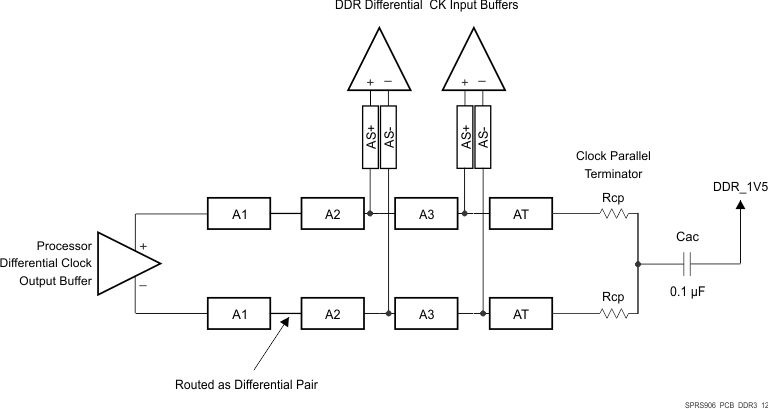
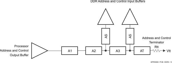
Figure 8-12 shows the topology of the CK net classes and Figure 8-13 shows the topology for the corresponding ADDR_CTRL net classes.
 Figure 8-12 CK Topology for Two DDR3 Devices
  Figure 8-13 ADDR_CTRL Topology for Two DDR3 Devices