ZHCSIM5F December 2016 – July 2018 AM5746 , AM5748 , AM5749
ADVANCE INFORMATION for pre-production products; subject to change without notice.
- 1器件概述
- 2修订历史记录
- 3Device Comparison
-
4Terminal Configuration and Functions
- 4.1 Pin Diagram
- 4.2 Pin Attributes
- 4.3
Signal Descriptions
- 4.3.1 VIP
- 4.3.2 DSS
- 4.3.3 HDMI
- 4.3.4 EMIF
- 4.3.5 GPMC
- 4.3.6 Timer
- 4.3.7 I2C
- 4.3.8 HDQ1W
- 4.3.9 UART
- 4.3.10 McSPI
- 4.3.11 QSPI
- 4.3.12 McASP
- 4.3.13 USB
- 4.3.14 SATA
- 4.3.15 PCIe
- 4.3.16 DCAN and MCAN
- 4.3.17 GMAC_SW
- 4.3.18 MLB
- 4.3.19 eMMC/SD/SDIO
- 4.3.20 GPIO
- 4.3.21 KBD
- 4.3.22 PWM
- 4.3.23 PRU-ICSS
- 4.3.24 Test Interfaces
- 4.3.25 System and Miscellaneous
- 4.4 Pin Multiplexing
- 4.5 Connections for Unused Pins
-
5Specifications
- 5.1 Absolute Maximum Ratings
- 5.2 ESD Ratings
- 5.3 Power-On Hours (POH) Limits
- 5.4 Recommended Operating Conditions
- 5.5 Operating Performance Points
- 5.6 Power Consumption Summary
- 5.7
Electrical Characteristics
- Table 5-7 LVCMOS DDR DC Electrical Characteristics
- Table 5-8 Dual Voltage LVCMOS I2C DC Electrical Characteristics
- Table 5-9 IQ1833 Buffers DC Electrical Characteristics
- Table 5-10 IHHV1833 Buffers DC Electrical Characteristics
- Table 5-11 LVCMOS OSC Buffers DC Electrical Characteristics
- Table 5-12 BC1833IHHV Buffers DC Electrical Characteristics
- Table 5-13 Dual Voltage SDIO1833 DC Electrical Characteristics
- Table 5-14 Dual Voltage LVCMOS DC Electrical Characteristics
- 5.7.1 HDMIPHY DC Electrical Characteristics
- 5.7.2 USBPHY DC Electrical Characteristics
- 5.7.3 SATAPHY DC Electrical Characteristics
- 5.7.4 PCIEPHY DC Electrical Characteristics
- 5.8 VPP Specifications for One-Time Programmable (OTP) eFuses
- 5.9 Thermal Characteristics
- 5.10
Timing Requirements and Switching Characteristics
- 5.10.1 Timing Parameters and Information
- 5.10.2 Interface Clock Specifications
- 5.10.3 Power Supply Sequences
- 5.10.4 Clock Specifications
- 5.10.5 Recommended Clock and Control Signal Transition Behavior
- 5.10.6
Peripherals
- 5.10.6.1 Timing Test Conditions
- 5.10.6.2 Virtual and Manual I/O Timing Modes
- 5.10.6.3 VIP
- 5.10.6.4 DSS
- 5.10.6.5 HDMI
- 5.10.6.6 EMIF
- 5.10.6.7 GPMC
- 5.10.6.8 I2C
- 5.10.6.9 HDQ1W
- 5.10.6.10 UART
- 5.10.6.11 McSPI
- 5.10.6.12 QSPI
- 5.10.6.13
McASP
- Table 5-79 Timing Requirements for McASP1
- Table 5-80 Timing Requirements for McASP2
- Table 5-81 Timing Requirements for McASP3/4/5/6/7/8
- Table 5-82 Switching Characteristics Over Recommended Operating Conditions for McASP1
- Table 5-83 Switching Characteristics Over Recommended Operating Conditions for McASP2
- Table 5-84 Switching Characteristics Over Recommended Operating Conditions for McASP3/4/5/6/7/8
- 5.10.6.14 USB
- 5.10.6.15 SATA
- 5.10.6.16 PCIe
- 5.10.6.17 CAN
- 5.10.6.18
GMAC_SW
- 5.10.6.18.1
GMAC MII Timings
- Table 5-98 Timing Requirements for miin_rxclk - MII Operation
- Table 5-99 Timing Requirements for miin_txclk - MII Operation
- Table 5-100 Timing Requirements for GMAC MIIn Receive 10/100 Mbit/s
- Table 5-101 Switching Characteristics Over Recommended Operating Conditions for GMAC MIIn Transmit 10/100 Mbits/s
- 5.10.6.18.2 GMAC MDIO Interface Timings
- 5.10.6.18.3
GMAC RMII Timings
- Table 5-106 Timing Requirements for GMAC REF_CLK - RMII Operation
- Table 5-107 Timing Requirements for GMAC RMIIn Receive
- Table 5-108 Switching Characteristics Over Recommended Operating Conditions for GMAC REF_CLK - RMII Operation
- Table 5-109 Switching Characteristics Over Recommended Operating Conditions for GMAC RMIIn Transmit 10/100 Mbits/s
- 5.10.6.18.4
GMAC RGMII Timings
- Table 5-113 Timing Requirements for rgmiin_rxc - RGMIIn Operation
- Table 5-114 Timing Requirements for GMAC RGMIIn Input Receive for 10/100/1000 Mbps
- Table 5-115 Switching Characteristics Over Recommended Operating Conditions for rgmiin_txctl - RGMIIn Operation for 10/100/1000 Mbit/s
- Table 5-116 Switching Characteristics for GMAC RGMIIn Output Transmit for 10/100/1000 Mbps
- 5.10.6.18.1
GMAC MII Timings
- 5.10.6.19
eMMC/SD/SDIO
- 5.10.6.19.1
MMC1—SD Card Interface
- 5.10.6.19.1.1 Default speed, 4-bit data, SDR, half-cycle
- 5.10.6.19.1.2 High speed, 4-bit data, SDR, half-cycle
- 5.10.6.19.1.3 SDR12, 4-bit data, half-cycle
- 5.10.6.19.1.4 SDR25, 4-bit data, half-cycle
- 5.10.6.19.1.5 UHS-I SDR50, 4-bit data, half-cycle
- 5.10.6.19.1.6 UHS-I SDR104, 4-bit data, half-cycle
- 5.10.6.19.1.7 UHS-I DDR50, 4-bit data
- 5.10.6.19.2 MMC2 — eMMC
- 5.10.6.19.3 MMC3 and MMC4—SDIO/SD
- 5.10.6.19.1
MMC1—SD Card Interface
- 5.10.6.20
PRU-ICSS
- 5.10.6.20.1 Programmable Real-Time Unit (PRU-ICSS PRU)
- 5.10.6.20.2
PRU-ICSS EtherCAT (PRU-ICSS ECAT)
- 5.10.6.20.2.1
PRU-ICSS ECAT Electrical Data and Timing
- Table 5-173 PRU-ICSS ECAT Timing Requirements – Input Validated With LATCH_IN
- Table 5-174 PRU-ICSS ECAT Timing Requirements – Input Validated With SYNCx
- Table 5-175 PRU-ICSS ECAT Timing Requirements – Input Validated With Start of Frame (SOF)
- Table 5-176 PRU-ICSS ECAT Timing Requirements - LATCHx_IN
- Table 5-177 PRU-ICSS ECAT Switching Requirements - Digital IOs
- 5.10.6.20.2.1
PRU-ICSS ECAT Electrical Data and Timing
- 5.10.6.20.3 PRU-ICSS MII_RT and Switch
- 5.10.6.20.4 PRU-ICSS Universal Asynchronous Receiver Transmitter (PRU-ICSS UART)
- 5.10.6.20.5 PRU-ICSS IOSETs
- 5.10.6.20.6 PRU-ICSS Manual Functional Mapping
- 5.10.6.21 System and Miscellaneous interfaces
- 5.10.7
Emulation and Debug Subsystem
- 5.10.7.1
JTAG
- 5.10.7.1.1
JTAG Electrical Data/Timing
- Table 5-209 Timing Requirements for IEEE 1149.1 JTAG
- Table 5-210 Switching Characteristics Over Recommended Operating Conditions for IEEE 1149.1 JTAG
- Table 5-211 Timing Requirements for IEEE 1149.1 JTAG With RTCK
- Table 5-212 Switching Characteristics Over Recommended Operating Conditions for IEEE 1149.1 JTAG With RTCK
- 5.10.7.1.1
JTAG Electrical Data/Timing
- 5.10.7.2 TPIU
- 5.10.7.1
JTAG
-
6Detailed Description
- 6.1 Description
- 6.2 Functional Block Diagram
- 6.3 MPU
- 6.4 DSP Subsystem
- 6.5 IVA
- 6.6 EVE
- 6.7 IPU
- 6.8 VPE
- 6.9 GPU
- 6.10 PRU-ICSS
- 6.11 Memory Subsystem
- 6.12 Interprocessor Communication
- 6.13 Interrupt Controller
- 6.14 EDMA
- 6.15 Peripherals
- 6.16 On-Chip Debug
-
7Applications, Implementation, and Layout
- 7.1 Power Supply Mapping
- 7.2
DDR3 Board Design and Layout Guidelines
- 7.2.1 DDR3 General Board Layout Guidelines
- 7.2.2
DDR3 Board Design and Layout Guidelines
- 7.2.2.1 Board Designs
- 7.2.2.2 DDR3 EMIFs
- 7.2.2.3 DDR3 Device Combinations
- 7.2.2.4 DDR3 Interface Schematic
- 7.2.2.5 Compatible JEDEC DDR3 Devices
- 7.2.2.6 PCB Stackup
- 7.2.2.7 Placement
- 7.2.2.8 DDR3 Keepout Region
- 7.2.2.9 Bulk Bypass Capacitors
- 7.2.2.10 High-Speed Bypass Capacitors
- 7.2.2.11 Net Classes
- 7.2.2.12 DDR3 Signal Termination
- 7.2.2.13 VREF_DDR Routing
- 7.2.2.14 VTT
- 7.2.2.15 CK and ADDR_CTRL Topologies and Routing Definition
- 7.2.2.16 Data Topologies and Routing Definition
- 7.2.2.17 Routing Specification
- 7.3 High Speed Differential Signal Routing Guidance
- 7.4 Power Distribution Network Implementation Guidance
- 7.5 Thermal Solution Guidance
- 7.6 Single-Ended Interfaces
- 7.7 LJCB_REFN/P Connections
- 7.8 Clock Routing Guidelines
- 8Device and Documentation Support
- 9Mechanical Packaging and Orderable Information
5.10.6.12 QSPI
The Quad SPI (QSPI) module is a type of SPI module that allows single, dual or quad read access to external SPI devices. This module has a memory mapped register interface, which provides a direct interface for accessing data from external SPI devices and thus simplifying software requirements. It works as a master only. There is one QSPI module in the device and it is primary intended for fast booting from quad-SPI flash memories.
General SPI features:
- Programmable clock divider
- Six pin interface (DCLK, CS_N, DOUT, DIN, QDIN1, QDIN2)
- 4 external chip select signals
- Support for 3-, 4- or 6-pin SPI interface
- Programmable CS_N to DOUT delay from 0 to 3 DCLKs
- Programmable signal polarities
- Programmable active clock edge
- Software controllable interface allowing for any type of SPI transfer
NOTE
For more information, see the Quad Serial Peripheral Interface section of the Device TRM.
CAUTION
The IO Timings provided in this section are only valid for some QSPI usage modes when the corresponding Virtual IO Timings or Manual IO Timings are configured as described in the tables found in this section.
CAUTION
The IO Timings provided in this section are only valid when all QSPI Chip Selects used in a system are configured to use the same Clock Mode (either Clock Mode 0 or Clock Mode3).
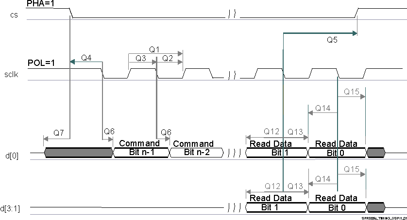
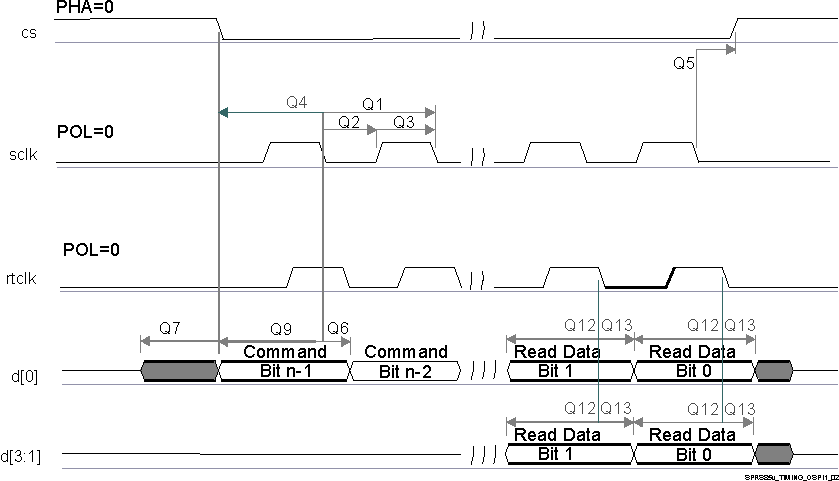
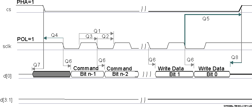
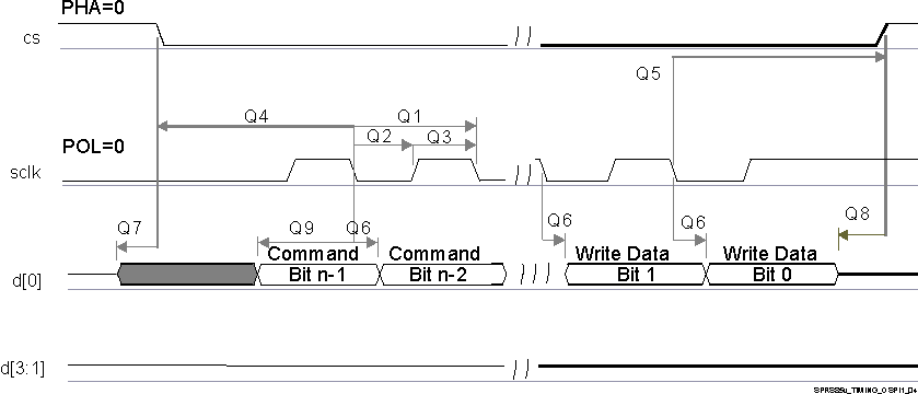
Table 5-76 and Table 5-77 present Timing and Switching Characteristics for Quad SPI Interface.
Table 5-76 Switching Characteristics for QSPI
| No | PARAMETER | DESCRIPTION | Mode | MIN | MAX | UNIT |
|---|---|---|---|---|---|---|
| Q1 | tc(SCLK) | Cycle time, sclk | Manual IO Timing Modes, Clock Mode 0 | 10.41 | ns | |
| Manual IO Timing Modes, Clock Mode 3 | 13.02 | ns | ||||
| Bootmode, Clock Mode 3 | 20.8 | |||||
| Q2 | tw(SCLKL) | Pulse duration, sclk low | All | Y*P-1 (1) | ns | |
| Q3 | tw(SCLKH) | Pulse duration, sclk high | All | Y*P-1 (1) | ns | |
| Q4 | td(CS-SCLK) | Delay time, sclk falling edge to cs active edge, CS3:0 | Manual IO Timing Modes | -M*P-1 (2)(3) | -M*P+2 (2)(3) | ns |
| Bootmode | -M*P-2.5 (2)(3) | -M*P+2.5 (2)(3) | ||||
| Q5 | td(SCLK-CS) | Delay time, sclk falling edge to cs inactive edge, CS3:0 | Manual IO Timing Modes | N*P-1 (2)(3) | N*P+2 (2)(3) | ns |
| Bootmode | N*P-2.5 (2)(3) | N*P+2.5 (2)(3) | ||||
| Q6 | td(SCLK-D1) | Delay time, sclk falling edge to d[0] transition | Manual IO Timing Modes | -1 | 2 | ns |
| Bootmode | -2.5 | 2.5 | ||||
| Q7 | tena(CS-D1LZ) | Enable time, cs active edge to d[0] driven (lo-z) | All | -P-3.5 | -P+2.5 | ns |
| Q8 | tdis(CS-D1Z) | Disable time, cs active edge to d[0] tri-stated (hi-z) | All | -P-2.5 | -P+2.0 | ns |
| Q9 | td(SCLK-D0) | Delay time, sclk first falling edge to first d[0] transition | Manual IO Timing Modes, PHA=0 Only | -1-P | 2-P | ns |
| Bootmode, PHA=0 Only | -2.5-P | 2.5-P |
- The Y parameter is defined as follows:
If DCLK_DIV is 0 or ODD then, Y equals 0.5.
If DCLK_DIV is EVEN then, Y equals (DCLK_DIV / 2) / (DCLK_DIV + 1).
For best performance, it is recommended to use a DCLK_DIV of 0 or ODD to minimize the duty cycle distortion. The HSDIVIDER on CLKOUTX2_H13 output of DPLL_PER can be used to achieve the desired clock divider ratio. All required details about clock division factor DCLK_DIV can be found in the Device TRM. - P = SCLK period.
- M = QSPI_SPI_DC_REG.DDx + 1 when Clock Mode 0.
M = QSPI_SPI_DC_REG.DDx when Clock Mode 3.
N = 2 when Clock Mode 0.
N = 3 when Clock Mode 3.
 Figure 5-53 QSPI Read (Clock Mode 3)
  Figure 5-54 QSPI Read (Clock Mode 0)
 CAUTION
The IO Timings provided in this section are only valid for some QSPI usage modes when the corresponding Virtual IO Timings or Manual IO Timings are configured as described in the tables found in this section.
Table 5-77 Timing Requirements for QSPI(2)(3)
| No | PARAMETER | DESCRIPTION | Mode | MIN | MAX | UNIT |
|---|---|---|---|---|---|---|
| Q12 | tsu(D-RTCLK) | Setup time, d[3:0] valid before falling rtclk edge | Manual IO Timing Modes, Clock Mode 0 | 2.9 | ns | |
| tsu(D-SCLK) | Setup time, d[3:0] valid before falling sclk edge | Manual IO Timing Modes, Clock Mode 3 | 5.7 | ns | ||
| Boot Mode, Clock Mode 3 | 12.3 | ns | ||||
| Q13 | th(RTCLK-D) | Hold time, d[3:0] valid after falling rtclk edge | Manual IO Timing Mode, Clock Mode 0 | -0.1 | ns | |
| th(SCLK-D) | Hold time, d[3:0] valid after falling sclk edge | Manual IO Timing Mode, Clock Mode 3 | 0.1 | ns | ||
| Boot Mode, Clock Mode 3 | 0.1 | ns | ||||
| Q14 | tsu(D-SCLK) | Setup time, final d[3:0] bit valid before final falling sclk edge | Manual IO Timing Mode, Clock Mode 3 | 5.7-P (1) | ns | |
| Boot Mode, Clock Mode 3 | 12.3-P (1) | ns | ||||
| Q15 | th(SCLK-D) | Hold time, final d[3:0] bit valid after final falling sclk edge | Manual IO Timing Mode, Clock Mode 3 | 0.1+P (1) | ns | |
| Boot Mode, Clock Mode 3 | 0.1+P (1) | ns |
- P = SCLK period.
- Clock Modes 1 and 2 are not supported.
- The Device captures data on the falling clock edge in Clock Mode 0 and 3, as opposed to the traditional rising clock edge. Although non-standard, the falling-edge-based setup and hold time timings have been designed to be compatible with standard SPI devices that launch data on the falling edge in Clock Modes 0 and 3.
 Figure 5-55 QSPI Write (Clock Mode 3)
  Figure 5-56 QSPI Write (Clock Mode 0)
 NOTE
To configure the desired Manual IO Timing Mode the user must follow the steps described in section Manual IO Timing Modes of the Device TRM.
The associated registers to configure are listed in the CFG REGISTER column. For more information, see chapter Control Module of the Device TRM.
Manual IO Timings Modes must be used to guarantee some IO timings for QSPI. See Table 5-33, Modes Summary for a list of IO timings requiring the use of Manual IO Timings Modes. See Table 5-78, Manual Functions Mapping for QSPI for a definition of the Manual modes.
Table 5-78 lists the A_DELAY and G_DELAY values needed to calculate the correct values to be set in the CFG_x registers.
Table 5-78 Manual Functions Mapping for QSPI
| BALL | BALL NAME | QSPI_MODE0_MANUAL1 | QSPI_MODE3_MANUAL1 | CFG REGISTER | MUXMODE | ||
|---|---|---|---|---|---|---|---|
| A_DELAY (ps) | G_DELAY (ps) | A_DELAY (ps) | G_DELAY (ps) | 1 | |||
| R3 | gpmc_a13 | 0 | 0 | 0 | 0 | CFG_GPMC_A13_IN | qspi1_rtclk |
| T2 | gpmc_a14 | 2149 | 1052 | 0 | 0 | CFG_GPMC_A14_IN | qspi1_d3 |
| U2 | gpmc_a15 | 2121 | 997 | 0 | 0 | CFG_GPMC_A15_IN | qspi1_d2 |
| U1 | gpmc_a16 | 2159 | 1134 | 0 | 0 | CFG_GPMC_A16_IN | qspi1_d0 |
| U1 | gpmc_a16 | 0 | 0 | 0 | 0 | CFG_GPMC_A16_OUT | qspi1_d0 |
| P3 | gpmc_a17 | 2135 | 1085 | 0 | 0 | CFG_GPMC_A17_IN | qspi1_d1 |
| R2 | gpmc_a18 | 0 | 0 | 151 | 0 | CFG_GPMC_A18_OUT | qspi1_sclk |
| T7 | gpmc_a3 | 0 | 0 | 0 | 0 | CFG_GPMC_A3_OUT | qspi1_cs2 |
| P6 | gpmc_a4 | 0 | 0 | 0 | 0 | CFG_GPMC_A4_OUT | qspi1_cs3 |
| P2 | gpmc_cs2 | 0 | 0 | 0 | 0 | CFG_GPMC_CS2_OUT | qspi1_cs0 |
| P1 | gpmc_cs3 | 0 | 0 | 22 | 0 | CFG_GPMC_CS3_OUT | qspi1_cs1 |