ZHCSSS9A march   2023  – august 2023 AM62A3 , AM62A3-Q1 , AM62A7 , AM62A7-Q1

PRODUCTION DATA  

  1.   1
  2. 特性
  3. 应用
  4. 说明
    1. 3.1 Functional Block Diagram
  5. Revision History
  6. Device Comparison
    1. 5.1 Related Products
  7. Terminal Configuration and Functions
    1. 6.1 Pin Diagrams
    2. 6.2 Pin Attributes
      1.      12
      2.      13
    3. 6.3 Signal Descriptions
      1.      15
      2. 6.3.1  CPSW3G
        1. 6.3.1.1 MAIN Domain
          1.        18
          2.        19
          3.        20
          4.        21
      3. 6.3.2  CPTS
        1. 6.3.2.1 MAIN Domain
          1.        24
      4. 6.3.3  CSI-2
        1. 6.3.3.1 MAIN Domain
          1.        27
      5. 6.3.4  DDRSS
        1. 6.3.4.1 MAIN Domain
          1.        30
      6. 6.3.5  DSS
        1. 6.3.5.1 MAIN Domain
          1.        33
      7. 6.3.6  ECAP
        1. 6.3.6.1 MAIN Domain
          1.        36
          2.        37
          3.        38
      8. 6.3.7  Emulation and Debug
        1. 6.3.7.1 MAIN Domain
          1.        41
        2. 6.3.7.2 MCU Domain
          1.        43
      9. 6.3.8  EPWM
        1. 6.3.8.1 MAIN Domain
          1.        46
          2.        47
          3.        48
          4.        49
      10. 6.3.9  EQEP
        1. 6.3.9.1 MAIN Domain
          1.        52
          2.        53
          3.        54
      11. 6.3.10 GPIO
        1. 6.3.10.1 MAIN Domain
          1.        57
          2.        58
        2. 6.3.10.2 MCU Domain
          1.        60
      12. 6.3.11 GPMC
        1. 6.3.11.1 MAIN Domain
          1.        63
      13. 6.3.12 I2C
        1. 6.3.12.1 MAIN Domain
          1.        66
          2.        67
          3.        68
          4.        69
        2. 6.3.12.2 MCU Domain
          1.        71
        3. 6.3.12.3 WKUP Domain
          1.        73
      14. 6.3.13 MCAN
        1. 6.3.13.1 MAIN Domain
          1.        76
        2. 6.3.13.2 MCU Domain
          1.        78
          2.        79
      15. 6.3.14 MCASP
        1. 6.3.14.1 MAIN Domain
          1.        82
          2.        83
          3.        84
      16. 6.3.15 MCSPI
        1. 6.3.15.1 MAIN Domain
          1.        87
          2.        88
          3.        89
        2. 6.3.15.2 MCU Domain
          1.        91
          2.        92
      17. 6.3.16 MDIO
        1. 6.3.16.1 MAIN Domain
          1.        95
      18. 6.3.17 MMC
        1. 6.3.17.1 MAIN Domain
          1.        98
          2.        99
          3.        100
      19. 6.3.18 OSPI
        1. 6.3.18.1 MAIN Domain
          1.        103
      20. 6.3.19 Power Supply
        1.       105
      21. 6.3.20 Reserved
        1.       107
      22. 6.3.21 System and Miscellaneous
        1. 6.3.21.1 Boot Mode Configuration
          1. 6.3.21.1.1 MAIN Domain
            1.         111
        2. 6.3.21.2 Clock
          1. 6.3.21.2.1 MCU Domain
            1.         114
          2. 6.3.21.2.2 WKUP Domain
            1.         116
        3. 6.3.21.3 System
          1. 6.3.21.3.1 MAIN Domain
            1.         119
          2. 6.3.21.3.2 MCU Domain
            1.         121
          3. 6.3.21.3.3 WKUP Domain
            1.         123
        4. 6.3.21.4 VMON
          1.        125
      23. 6.3.22 TIMER
        1. 6.3.22.1 MAIN Domain
          1.        128
        2. 6.3.22.2 MCU Domain
          1.        130
        3. 6.3.22.3 WKUP Domain
          1.        132
      24. 6.3.23 UART
        1. 6.3.23.1 MAIN Domain
          1.        135
          2.        136
          3.        137
          4.        138
          5.        139
          6.        140
          7.        141
        2. 6.3.23.2 MCU Domain
          1.        143
        3. 6.3.23.3 WKUP Domain
          1.        145
      25. 6.3.24 USB
        1. 6.3.24.1 MAIN Domain
          1.        148
          2.        149
    4. 6.4 Pin Connectivity Requirements
  8. Specifications
    1. 7.1  Absolute Maximum Ratings
    2. 7.2  ESD Ratings
    3. 7.3  Power-On Hours (POH)
    4. 7.4  Recommended Operating Conditions
    5. 7.5  Operating Performance Points
    6. 7.6  Power Consumption Summary
    7. 7.7  Electrical Characteristics
      1. 7.7.1 I2C Open-Drain, and Fail-Safe (I2C OD FS) Electrical Characteristics
      2. 7.7.2 Fail-Safe Reset (FS RESET) Electrical Characteristics
      3. 7.7.3 High-Frequency Oscillator (HFOSC) Electrical Characteristics
      4. 7.7.4 Low-Frequency Oscillator (LFXOSC) Electrical Characteristics
      5. 7.7.5 SDIO Electrical Characteristics
      6. 7.7.6 LVCMOS Electrical Characteristics
      7. 7.7.7 CSI-2 (D-PHY) Electrical Characteristics
      8. 7.7.8 USB2PHY Electrical Characteristics
      9. 7.7.9 DDR Electrical Characteristics
    8. 7.8  VPP Specifications for One-Time Programmable (OTP) eFuses
      1. 7.8.1 Recommended Operating Conditions for OTP eFuse Programming
      2. 7.8.2 Hardware Requirements
      3. 7.8.3 Programming Sequence
      4. 7.8.4 Impact to Your Hardware Warranty
    9. 7.9  Thermal Resistance Characteristics
      1. 7.9.1 Thermal Resistance Characteristics for AMB Package
    10. 7.10 Timing and Switching Characteristics
      1. 7.10.1 Timing Parameters and Information
      2. 7.10.2 Power Supply Requirements
        1. 7.10.2.1 Power Supply Slew Rate Requirement
        2. 7.10.2.2 Power Supply Sequencing
          1. 7.10.2.2.1 Power-Up Sequencing
          2. 7.10.2.2.2 Power-Down Sequencing
          3. 7.10.2.2.3 Partial IO Power Sequencing
      3. 7.10.3 System Timing
        1. 7.10.3.1 Reset Timing
        2. 7.10.3.2 Error Signal Timing
        3. 7.10.3.3 Clock Timing
      4. 7.10.4 Clock Specifications
        1. 7.10.4.1 Input Clocks / Oscillators
          1. 7.10.4.1.1 MCU_OSC0 Internal Oscillator Clock Source
            1. 7.10.4.1.1.1 Load Capacitance
            2. 7.10.4.1.1.2 Shunt Capacitance
          2. 7.10.4.1.2 MCU_OSC0 LVCMOS Digital Clock Source
          3. 7.10.4.1.3 WKUP_LFOSC0 Internal Oscillator Clock Source
          4. 7.10.4.1.4 WKUP_LFOSC0 LVCMOS Digital Clock Source
          5. 7.10.4.1.5 WKUP_LFOSC0 Not Used
        2. 7.10.4.2 Output Clocks
        3. 7.10.4.3 PLLs
        4. 7.10.4.4 Recommended System Precautions for Clock and Control Signal Transitions
      5. 7.10.5 Peripherals
        1. 7.10.5.1  CPSW3G
          1. 7.10.5.1.1 CPSW3G MDIO Timing
          2. 7.10.5.1.2 CPSW3G RMII Timing
          3. 7.10.5.1.3 CPSW3G RGMII Timing
        2. 7.10.5.2  CPTS
        3. 7.10.5.3  CSI-2
        4. 7.10.5.4  DDRSS
        5. 7.10.5.5  DSS
        6. 7.10.5.6  ECAP
        7. 7.10.5.7  Emulation and Debug
          1. 7.10.5.7.1 Trace
          2. 7.10.5.7.2 JTAG
        8. 7.10.5.8  EPWM
        9. 7.10.5.9  EQEP
        10. 7.10.5.10 GPIO
        11. 7.10.5.11 GPMC
          1. 7.10.5.11.1 GPMC and NOR Flash — Synchronous Mode
          2. 7.10.5.11.2 GPMC and NOR Flash — Asynchronous Mode
          3. 7.10.5.11.3 GPMC and NAND Flash — Asynchronous Mode
        12. 7.10.5.12 I2C
        13. 7.10.5.13 MCAN
        14. 7.10.5.14 MCASP
        15. 7.10.5.15 MCSPI
          1. 7.10.5.15.1 MCSPI — Controller Mode
          2. 7.10.5.15.2 MCSPI — Peripheral Mode
        16. 7.10.5.16 MMCSD
          1. 7.10.5.16.1 MMC0 - eMMC/SD/SDIO Interface
            1. 7.10.5.16.1.1  Legacy SDR Mode
            2. 7.10.5.16.1.2  High Speed SDR Mode
            3. 7.10.5.16.1.3  HS200 Mode
            4. 7.10.5.16.1.4  Default Speed Mode
            5. 7.10.5.16.1.5  High Speed Mode
            6. 7.10.5.16.1.6  UHS–I SDR12 Mode
            7. 7.10.5.16.1.7  UHS–I SDR25 Mode
            8. 7.10.5.16.1.8  UHS–I SDR50 Mode
            9. 7.10.5.16.1.9  UHS–I DDR50 Mode
            10. 7.10.5.16.1.10 UHS–I SDR104 Mode
          2. 7.10.5.16.2 MMC1/MMC2 - SD/SDIO Interface
            1. 7.10.5.16.2.1 Default Speed Mode
            2. 7.10.5.16.2.2 High Speed Mode
            3. 7.10.5.16.2.3 UHS–I SDR12 Mode
            4. 7.10.5.16.2.4 UHS–I SDR25 Mode
            5. 7.10.5.16.2.5 UHS–I SDR50 Mode
            6. 7.10.5.16.2.6 UHS–I DDR50 Mode
            7. 7.10.5.16.2.7 UHS–I SDR104 Mode
        17. 7.10.5.17 OSPI
          1. 7.10.5.17.1 OSPI0 PHY Mode
            1. 7.10.5.17.1.1 OSPI0 With PHY Data Training
            2. 7.10.5.17.1.2 OSPI0 Without Data Training
              1. 7.10.5.17.1.2.1 OSPI0 PHY SDR Timing
              2. 7.10.5.17.1.2.2 OSPI0 PHY DDR Timing
          2. 7.10.5.17.2 OSPI0 Tap Mode
            1. 7.10.5.17.2.1 OSPI0 Tap SDR Timing
            2. 7.10.5.17.2.2 OSPI0 Tap DDR Timing
        18. 7.10.5.18 Timers
        19. 7.10.5.19 UART
        20. 7.10.5.20 USB
  9. Detailed Description
    1. 8.1 Overview
    2. 8.2 Processor Subsystems
      1. 8.2.1 Arm Cortex-A53 Subsystem
      2. 8.2.2 Device/Power Manager
      3. 8.2.3 MCU Arm Cortex-R5F Subsystem
    3. 8.3 Accelerators and Coprocessors
      1. 8.3.1 C7xV-256 Deep Learning Accelerator
      2. 8.3.2 Vision Pre-processing Accelerator
      3. 8.3.3 JPEG Encoder
      4. 8.3.4 Video Accelerator
    4. 8.4 Other Subsystems
      1. 8.4.1 Dual Clock Comparator (DCC)
      2. 8.4.2 Data Movement Subsystem (DMSS)
      3. 8.4.3 Memory Cyclic Redundancy Check (MCRC)
      4. 8.4.4 Peripheral DMA Controller (PDMA)
      5. 8.4.5 Real-Time Clock (RTC)
    5. 8.5 Peripherals
      1. 8.5.1  Gigabit Ethernet Switch (CPSW3G)
      2. 8.5.2  Camera Serial Interface Receiver (CSI_RX_IF)
      3. 8.5.3  Display Subsystem (DSS)
      4. 8.5.4  Enhanced Capture (ECAP)
      5. 8.5.5  Error Location Module (ELM)
      6. 8.5.6  Enhanced Pulse Width Modulation (EPWM)
      7. 8.5.7  Error Signaling Module (ESM)
      8. 8.5.8  Enhanced Quadrature Encoder Pulse (EQEP)
      9. 8.5.9  General-Purpose Interface (GPIO)
      10. 8.5.10 General-Purpose Memory Controller (GPMC)
      11. 8.5.11 Global Timebase Counter (GTC)
      12. 8.5.12 Inter-Integrated Circuit (I2C)
      13. 8.5.13 Modular Controller Area Network (MCAN)
      14. 8.5.14 Multichannel Audio Serial Port (MCASP)
      15. 8.5.15 Multichannel Serial Peripheral Interface (MCSPI)
      16. 8.5.16 Multi-Media Card Secure Digital (MMCSD)
      17. 8.5.17 Octal Serial Peripheral Interface (OSPI)
      18. 8.5.18 Timers
      19. 8.5.19 Universal Asynchronous Receiver/Transmitter (UART)
      20. 8.5.20 Universal Serial Bus Subsystem (USBSS)
  10. Applications, Implementation, and Layout
    1. 9.1 Device Connection and Layout Fundamentals
      1. 9.1.1 Power Supply
        1. 9.1.1.1 Power Supply Designs
        2. 9.1.1.2 Power Distribution Network Implementation Guidance
      2. 9.1.2 External Oscillator
      3. 9.1.3 JTAG, EMU, and TRACE
      4. 9.1.4 Unused Pins
    2. 9.2 Peripheral- and Interface-Specific Design Information
      1. 9.2.1 DDR Board Design and Layout Guidelines
      2. 9.2.2 OSPI/QSPI/SPI Board Design and Layout Guidelines
        1. 9.2.2.1 No Loopback, Internal PHY Loopback, and Internal Pad Loopback
        2. 9.2.2.2 External Board Loopback
        3. 9.2.2.3 DQS (only available in Octal SPI devices)
      3. 9.2.3 USB VBUS Design Guidelines
      4. 9.2.4 System Power Supply Monitor Design Guidelines
      5. 9.2.5 High Speed Differential Signal Routing Guidance
      6. 9.2.6 Thermal Solution Guidance
    3. 9.3 Clock Routing Guidelines
      1. 9.3.1 Oscillator Routing
  11. 10Device and Documentation Support
    1. 10.1 Device Nomenclature
      1. 10.1.1 Standard Package Symbolization
      2. 10.1.2 Device Naming Convention
    2. 10.2 Tools and Software
    3. 10.3 Documentation Support
    4. 10.4 支持资源
    5. 10.5 Trademarks
    6. 10.6 静电放电警告
    7. 10.7 术语表
  12. 11Mechanical, Packaging, and Orderable Information
    1. 11.1 Packaging Information

封装选项

请参考 PDF 数据表获取器件具体的封装图。

机械数据 (封装 | 引脚)
  • AMB|484
散热焊盘机械数据 (封装 | 引脚)
订购信息
OSPI0 With PHY Data Training

Read and write data valid windows will shift due to variation in process, voltage, temperature, and operating frequency. A data training method may be implemented to dynamically configure optimal read and write timing. Implementing data training enables proper operation across temperature with a specific process, voltage, and frequency operating condition, while achieving a higher operating frequency.

Data transmit and receive timing parameters are not defined for the data training use case since they are dynamically adjusted based on the operating condition.

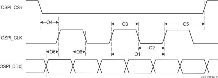
Table 7-111 defines DLL delays required for OSPI0 with Data Training. Table 7-112, Figure 7-94, Figure 7-95, Table 7-113, Figure 7-96, and Figure 7-97 present timing requirements and switching characteristics for OSPI0 with Data Training.

Table 7-111 OSPI0 DLL Delay Mapping for PHY Data Training
MODE OSPI_PHY_CONFIGURATION_REG BIT FIELD DELAY VALUE
Transmit
All modes PHY_CONFIG_TX_DLL_DELAY_FLD, (1)
Receive
All modes PHY_CONFIG_RX_DLL_DELAY_FLD (2)
Transmit DLL delay value determined by training software
Receive DLL delay value determined by training software
Table 7-112 OSPI0 Timing Requirements – PHY Data Training see Figure 7-94, and Figure 7-95
NO. MODE MIN MAX UNIT
O15 tsu(D-LBCLK) Setup time, OSPI0_D[7:0] valid before active OSPI0_DQS edge DDR with DQS (1) ns
O16 th(LBCLK-D) Hold time, OSPI0_D[7:0] valid after active OSPI0_DQS edge DDR with DQS (1) ns
O21 tsu(D-LBCLK) Setup time, OSPI0_D[7:0] valid before active OSPI0_DQS edge SDR with External Board Loopback (1) ns
O22 th(LBCLK-D) Hold time, OSPI0_D[7:0] valid after active OSPI0_DQS edge SDR with External Board Loopback (1) ns
tDVW Data valid window (O15 + O16) 1.8V, DDR with DQS 1.6 ns
3.3V, DDR with DQS 2.2 ns
Data valid window (O21 + O22) 1.8V, SDR with External Board Loopback 2.3 ns
3.3V, SDR with External Board Loopback 2.9 ns
Minimum setup and hold time requirements for OSPI0_D[7:0] inputs are not defined when Data Training is used to find the optimum data valid window. The tDVW parameter defines the minimum data invalid window required. This parameter is provided in lieu of minimum setup and minimum hold times, where it must be used to check compatibility with the data valid window provided by an attached device.
GUID-E00937AF-BFE0-4418-A9ED-E46A1C187641-low.gif Figure 7-94 OSPI0 Timing Requirements – PHY Data Training, DDR with DQS
GUID-695D8740-6CD5-423B-8BD1-C0767EA74058-low.gif Figure 7-95 OSPI0 Timing Requirements – PHY Data Training, SDR with External Board Loopback
Table 7-113 OSPI Switching Characteristics – PHY Data Training See Figure 7-96 and Figure 7-97
NO. PARAMETER MODE MIN MAX UNIT
O1 tc(CLK) Cycle time, OSPI0_CLK 1.8V, DDR 6.0 10 ns
3.3V, DDR 7.5 10 ns
O7 1.8V, SDR 6.0 10 ns
3.3V, SDR 7.5 10 ns
O2 tw(CLKL) Pulse duration, OSPI0_CLK low DDR ((0.475P(1)) - 0.3) ns
O8 SDR
O3 tw(CLKH) Pulse duration, OSPI0_CLK high DDR ((0.475P(1)) - 0.3) ns
O9 SDR
O4 td(CSn-CLK) Delay time, OSPI0_CSn[3:0] active edge to OSPI0_CLK rising edge DDR ((0.475P(1)) + (0.975M(2)R(4)) + (0.04TD(5)) - 1) ((0.525P(1)) + (1.025M(2)R(4)) + (0.11TD(5)) + 1) ns
O10 SDR
O5 td(CLK-CSn) Delay time, OSPI0_CLK rising edge to OSPI0_CSn[3:0] inactive edge DDR ((0.475P(1)) + (0.975N(3)R(4)) - (0.04TD(5)) - 1) ((0.525P(1)) + (1.025N(3)R(4)) - (0.11TD(5)) + 1) ns
O11 SDR
O6 td(CLK-D) Delay time, OSPI0_CLK active edge to OSPI0_D[7:0] transition DDR (6) (6) ns
O12 SDR
tDIVW Data invalid window (O6 Max - Min) DDR 1.6 ns
Data invalid window (O12 Max - Min) SDR
P = SCLK cycle time in ns = OSPI0_CLK cycle time in ns
M = OSPI_DEV_DELAY_REG[D_INIT_FLD]
N = OSPI_DEV_DELAY_REG[D_AFTER_FLD]
R = reference clock cycle time in ns
TD = PHY_CONFIG_TX_DLL_DELAY_FLD
Minimum and maximum delay times for OSPI0_D[7:0] outputs are not defined when Data Training is used to find the optimum data valid window. The tDIVW parameter defines the maximum data invalid window. This parameter is provided in lieu of minimum and maximum delay times, where it must be used to check compatibility with the data valid window requirements of an attached device.
GUID-489AADD3-03CA-408E-8257-98F0E65997F1-low.gif Figure 7-96 OSPI0 Switching Characteristics – PHY DDR Data Training
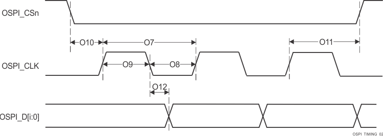
GUID-589F5F4F-35E6-44AA-9408-AC740E1F1B70-low.gif Figure 7-97 OSPI0 Switching Characteristics – PHY SDR Data Training