ZHCSLA7C December 2019 – September 2023 AM6526 , AM6528 , AM6546 , AM6548
PRODUCTION DATA
- 1
- 1 特性
- 2 应用
- 3 说明
- 4 Device Comparison
-
5 Terminal Configuration and Functions
- 5.1 Pin Diagram
- 5.2 Pin Attributes
- 5.3
Signal Descriptions
- 5.3.1 ADC
- 5.3.2 CAL
- 5.3.3 CPSW2G
- 5.3.4 DDRSS
- 5.3.5 DMTIMER
- 5.3.6 DSS
- 5.3.7 ECAP
- 5.3.8 EHRPWM
- 5.3.9 EQEP
- 5.3.10 GPIO
- 5.3.11 GPMC
- 5.3.12 HyperBus
- 5.3.13 I2C
- 5.3.14 MCAN
- 5.3.15 MCASP
- 5.3.16 MCSPI
- 5.3.17 MMCSD
- 5.3.18 CPTS
- 5.3.19 OLDI
- 5.3.20 OSPI
- 5.3.21 PRU_ICSSG
- 5.3.22 SERDES
- 5.3.23 UART
- 5.3.24 USB
- 5.3.25 Emulation and Debug
- 5.3.26 System and Miscellaneous
- 5.3.27 Power Supply
- 5.4 Pin Multiplexing
- 5.5 Connections for Unused Pins
-
6 Specifications
- 6.1 Absolute Maximum Ratings
- 6.2 ESD Ratings
- 6.3 Power-On Hours (POH)
- 6.4 Recommended Operating Conditions
- 6.5 Operating Performance Points
- 6.6
Electrical Characteristics
- 6.6.1 I2C OPEN DRAIN DC Electrical Characteristics
- 6.6.2 Analog OSC Buffers DC Electrical Characteristics
- 6.6.3 Analog ADC DC Electrical Characteristics
- 6.6.4 DPHY CSI2 Buffers DC Electrical Characteristics
- 6.6.5 OLDI LVDS Buffers DC Electrical Characteristics
- 6.6.6 USBHS Buffers DC Electrical Characteristics
- 6.6.7 SERDES Buffers DC Electrical Characteristics
- 6.7 VPP Specifications for One-Time Programmable (OTP) eFuses
- 6.8 Thermal Resistance Characteristics
- 6.9
Timing and Switching Characteristics
- 6.9.1 Timing Parameters and Information
- 6.9.2 Power Supply Sequencing
- 6.9.3 System Timing
- 6.9.4
Clock Specifications
- 6.9.4.1
Input Clocks / Oscillators
- 6.9.4.1.1 WKUP_OSC0 Internal Oscillator Clock Source
- 6.9.4.1.2 WKUP_OSC0 LVCMOS Digital Clock Source
- 6.9.4.1.3 Auxiliary OSC1 Internal Oscillator Clock Source
- 6.9.4.1.4 Auxiliary OSC1 LVCMOS Digital Clock Source
- 6.9.4.1.5 Auxiliary OSC1 Not Used
- 6.9.4.1.6 WKUP_LFOSC0 Internal Oscillator Clock Source
- 6.9.4.1.7 WKUP_LFOSC0 LVCMOS Digital Clock Source
- 6.9.4.1.8 WKUP_LFOSC0 Not Used
- 6.9.4.2 Output Clocks
- 6.9.4.3 PLLs
- 6.9.4.4 Recommended Clock and Control Signal Transition Behavior
- 6.9.4.5 Module and Peripheral Clock Frequencies
- 6.9.4.1
Input Clocks / Oscillators
- 6.9.5
Peripherals
- 6.9.5.1 VIN
- 6.9.5.2
CPSW2G
- 6.9.5.2.1 CPSW2G MDIO Interface Timings
- 6.9.5.2.2 CPSW2G RMII Timings
- 6.9.5.2.3
CPSW2G RGMII Timings
- 6.9.5.2.3.1 Timing Requirements for RGMII[x]_RCLK - RGMII Mode
- 6.9.5.2.3.2 Timing Requirements for RGMII[x]_RD[3:0], and RGMII[x]_RCTL - RGMII Mode
- 6.9.5.2.3.3 Switching Characteristics for RGMII[x]_TCLK - RGMII Mode
- 6.9.5.2.3.4 Switching Characteristics for RGMII[x]_TD[3:0], and RGMII[x]_TX_CTL - RGMII Mode
- 6.9.5.3 CSI2
- 6.9.5.4 DDRSS
- 6.9.5.5 DSS
- 6.9.5.6 eCAP
- 6.9.5.7 ePWM
- 6.9.5.8 eQEP
- 6.9.5.9 GPIO
- 6.9.5.10 GPMC
- 6.9.5.11 HyperBus
- 6.9.5.12 I2C
- 6.9.5.13 MCAN
- 6.9.5.14 MCASP
- 6.9.5.15 MCSPI
- 6.9.5.16 MMCSD
- 6.9.5.17 CPTS
- 6.9.5.18 OSPI
- 6.9.5.19 OLDI
- 6.9.5.20 PCIE
- 6.9.5.21
PRU_ICSSG
- 6.9.5.21.1
Programmable Real-Time Unit (PRU_ICSSG PRU)
- 6.9.5.21.1.1 PRU_ICSSG PRU Direct Input/Output Mode Electrical Data and Timing
- 6.9.5.21.1.2 PRU_ICSSG PRU Parallel Capture Mode Electrical Data and Timing
- 6.9.5.21.1.3 PRU_ICSSG PRU Shift Mode Electrical Data and Timing
- 6.9.5.21.1.4 PRU_ICSSG PRU Sigma Delta and Peripheral Interface Modes Electrical Data and Timing
- 6.9.5.21.2 PRU_ICSSG Pulse Width Modulation (PWM)
- 6.9.5.21.3 PRU_ICSSG Industrial Ethernet Peripheral (PRU_ICSSG IEP)
- 6.9.5.21.4 PRU_ICSSG Universal Asynchronous Receiver Transmitter (PRU-ICSS UART)
- 6.9.5.21.5 PRU_ICSSG Enhanced Capture Peripheral (PRU-ICSS ECAP)
- 6.9.5.21.6
PRU_ICSSG RGMII, MII_RT, and Switch
- 6.9.5.21.6.1 PRU_ICSSG MDIO Electrical Data and Timing
- 6.9.5.21.6.2
PRU_ICSSG RGMII Electrical Data and Timing
- 6.9.5.21.6.2.1 PRU_ICSSG RGMII Timing Requirements - RGMII_RXC
- 6.9.5.21.6.2.2 PRU_ICSSG RGMII Timing Requirements - RGMII_RD[3:0] and RGMII_RX_CTL
- 6.9.5.21.6.2.3 PRU_ICSSG RGMII Switching Characteristics - RGMII_TXC
- 6.9.5.21.6.2.4 PRU_ICSSG RGMII Switching Characteristics - RGMII_TD[3:0] and RGMII_TX_CTL
- 6.9.5.21.6.3
PRU_ICSSG MII_RT Electrical Data and Timing
- 6.9.5.21.6.3.1 PRU_ICSSG MII_RT Timing Requirements – MII_RX_CLK
- 6.9.5.21.6.3.2 PRU_ICSSG MII_RT Timing Requirements – MII_RXD[3:0], MII_RX_DV, and MII_RX_ER
- 6.9.5.21.6.3.3 PRU_ICSSG MII_RT Switching Characteristics – MII_TX_CLK
- 6.9.5.21.6.3.4 PRU_ICSSG MII_RT Switching Characteristics – MII_TXD[3:0] and MII_TXEN
- 6.9.5.21.1
Programmable Real-Time Unit (PRU_ICSSG PRU)
- 6.9.5.22 Timers
- 6.9.5.23 UART
- 6.9.5.24 USB
- 6.9.5.25 Emulation and Debug
-
7 Detailed Description
- 7.1 Overview
- 7.2 Processor Subsystems
- 7.3 Accelerators and Coprocessors
- 7.4
Other Subsystems
- 7.4.1 DMSC
- 7.4.2 MSMC
- 7.4.3 NAVSS
- 7.4.4 PDMA Controller
- 7.4.5
Peripherals
- 7.4.5.1 ADC
- 7.4.5.2 CAL
- 7.4.5.3 CPSW2G
- 7.4.5.4 DCC
- 7.4.5.5 DDRSS
- 7.4.5.6 DSS
- 7.4.5.7 ЕCAP
- 7.4.5.8 EPWM
- 7.4.5.9 ELM
- 7.4.5.10 ESM
- 7.4.5.11 EQEP
- 7.4.5.12 GPIO
- 7.4.5.13 GPMC
- 7.4.5.14 HyperBus
- 7.4.5.15 I2C
- 7.4.5.16 MCAN
- 7.4.5.17 MCASP
- 7.4.5.18 MCRC
- 7.4.5.19 MCSPI
- 7.4.5.20 MMCSD
- 7.4.5.21 OSPI
- 7.4.5.22 PCIE
- 7.4.5.23 SerDes
- 7.4.5.24 RTI
- 7.4.5.25 Timers
- 7.4.5.26 UART
- 7.4.5.27 USB
- 7.5 Identification
- 7.6 Boot Modes
-
8 Applications, Implementation, and Layout
- 8.1 Device Connection and Layout Fundamentals
- 8.2
Peripheral- and Interface-Specific Design Information
- 8.2.1 DDR Board Design and Layout Guidelines
- 8.2.2 OSPI Board Design and Layout Guidelines
- 8.2.3 USB Design Guidelines
- 8.2.4 High Speed Differential Signal Routing Guidance
- 8.2.5 System Power Supply Monitor Design Guidelines
- 8.2.6 MMC Design Guidelines
- 8.2.7 Integrated Power Management Features
- 8.2.8 External Capacitors
- 8.2.9 Thermal Solution Guidance
- 9 Device and Documentation Support
- 10Revision History
- 11Mechanical, Packaging, and Orderable Information
6.9.5.10.2.2 GPMC and NOR Flash Switching Characteristics—Asynchronous Mode
| NO. | PARAMETER | DESCRIPTION | MODE(15) | MIN | MAX | UNIT |
|---|---|---|---|---|---|---|
| FA0 | tw(be[x]nV) | Pulse duration, output lower-byte enable and command latch enable GPMC_BE0n_CLE, output upper-byte enable GPMC_BE1n valid time | Read | 0+N (12) | ns | |
| Write | 0+N (12) | |||||
| FA1 | tw(csnV) | Pulse duration, output chip select GPMC_CSn[x](13) low | Read | 0+A (1) | ns | |
| Write | 0+A (1) | |||||
| FA3 | td(csnV-advnIV) | Delay time, output chip select GPMC_CSn[x](13) valid to output address valid and address latch enable GPMC_ADVn_ALE invalid | Read | -2+B (2) | 2+B (2) | ns |
| Write | -2+B (2) | 2+B (2) | ||||
| FA4 | td(csnV-oenIV) | Delay time, output chip select GPMC_CSn[x](13) valid to output enable GPMC_OEn_REn invalid (Single read) | div_by_1_mode; GPMC_FCLK_MUX_133; TIMEPARAGRANULARITY_X1 | -2+C (3) | 2+C (3) | ns |
| FA9 | td(aV-csnV) | Delay time, output address GPMC_A[27:1] valid to output chip select GPMC_CSn[x](13) valid | div_by_1_mode; GPMC_FCLK_MUX_133; TIMEPARAGRANULARITY_X1 | -2+J (9) | 2+J (9) | ns |
| FA10 | td(be[x]nV-csnV) | Delay time, output lower-byte enable and command latch enable GPMC_BE0n_CLE, output upper-byte enable GPMC_BE1n valid to output chip select GPMC_CSn[x](13) valid | div_by_1_mode; GPMC_FCLK_MUX_133; TIMEPARAGRANULARITY_X1 | -2+J (9) | 2+J (9) | ns |
| FA12 | td(csnV-advnV) | Delay time, output chip select GPMC_CSn[x](13) valid to output address valid and address latch enable GPMC_ADVn_ALE valid | div_by_1_mode; GPMC_FCLK_MUX_133; TIMEPARAGRANULARITY_X1 | -2+K (10) | 2+K (10) | ns |
| FA13 | td(csnV-oenV) | Delay time, output chip select GPMC_CSn[x](13) valid to output enable GPMC_OEn_REn valid | div_by_1_mode; GPMC_FCLK_MUX_133; TIMEPARAGRANULARITY_X1 | -2+L (11) | 2+L (11) | ns |
| FA16 | tw(aIV) | Pulse duration output address GPMC_A[26:1] invalid between 2 successive read and write accesses | div_by_1_mode; GPMC_FCLK_MUX_133; TIMEPARAGRANULARITY_X1 | 0+G (7) | ns | |
| FA18 | td(csnV-oenIV) | Delay time, output chip select GPMC_CSn[x](13) valid to output enable GPMC_OEn_REn invalid (Burst read) | div_by_1_mode; GPMC_FCLK_MUX_133; TIMEPARAGRANULARITY_X1 | -2+I (8) | 2+I (8) | ns |
| FA20 | tw(aV) | Pulse duration, output address GPMC_A[27:1] valid - 2nd, 3rd, and 4th accesses | div_by_1_mode; GPMC_FCLK_MUX_133; TIMEPARAGRANULARITY_X1 | 0+D (4) | ns | |
| FA25 | td(csnV-wenV) | Delay time, output chip select GPMC_CSn[x](13) valid to output write enable GPMC_WEn valid | div_by_1_mode; GPMC_FCLK_MUX_133; TIMEPARAGRANULARITY_X1 | -2+E (5) | 2+E (5) | ns |
| FA27 | td(csnV-wenIV) | Delay time, output chip select GPMC_CSn[x](13) valid to output write enable GPMC_WEn invalid | div_by_1_mode; GPMC_FCLK_MUX_133; TIMEPARAGRANULARITY_X1 | -2+F (6) | 2+F (6) | ns |
| FA28 | td(wenV-dV) | Delay time, output write enable GPMC_WEn valid to output data GPMC_AD[15:0] valid | div_by_1_mode; GPMC_FCLK_MUX_133; TIMEPARAGRANULARITY_X1 | 2.8 | ns | |
| FA29 | td(dV-csnV) | Delay time, output data GPMC_AD[15:0] valid to output chip select GPMC_CSn[x](13) valid | div_by_1_mode; GPMC_FCLK_MUX_133; TIMEPARAGRANULARITY_X1 | -2+J (9) | 2+J (9) | ns |
| FA37 | td(oenV-aIV) | Delay time, output enable GPMC_OEn_REn valid to output address GPMC_AD[15:0] phase end | div_by_1_mode; GPMC_FCLK_MUX_133; TIMEPARAGRANULARITY_X1 | 2.8 | ns |
(1) For single read: A = (CSRdOffTime - CSOnTime) × (TimeParaGranularity + 1) × GPMC_FCLK(14)
For single write: A = (CSWrOffTime - CSOnTime) × (TimeParaGranularity + 1) × GPMC_FCLK(14)
For burst read: A = (CSRdOffTime - CSOnTime + (n - 1) × PageBurstAccessTime) × (TimeParaGranularity + 1) × GPMC_FCLK(14)
For burst write: A = (CSWrOffTime - CSOnTime + (n - 1) × PageBurstAccessTime) × (TimeParaGranularity + 1) × GPMC_FCLK(14)
with n being the page burst access number
(2) For reading: B = ((ADVRdOffTime - CSOnTime) × (TimeParaGranularity + 1) + 0.5 × (ADVExtraDelay - CSExtraDelay)) × GPMC_FCLK(14)
For writing: B = ((ADVWrOffTime - CSOnTime) × (TimeParaGranularity + 1) + 0.5 × (ADVExtraDelay - CSExtraDelay)) × GPMC_FCLK(14)
For writing: B = ((ADVWrOffTime - CSOnTime) × (TimeParaGranularity + 1) + 0.5 × (ADVExtraDelay - CSExtraDelay)) × GPMC_FCLK(14)
(3) C = ((OEOffTime - CSOnTime) × (TimeParaGranularity + 1) + 0.5 × (OEExtraDelay - CSExtraDelay)) × GPMC_FCLK(14)
(4) D = PageBurstAccessTime × (TimeParaGranularity + 1) × GPMC_FCLK(14)
(5) E = ((WEOnTime - CSOnTime) × (TimeParaGranularity + 1) + 0.5 × (WEExtraDelay - CSExtraDelay)) × GPMC_FCLK(14)
(6) F = ((WEOffTime - CSOnTime) × (TimeParaGranularity + 1) + 0.5 × (WEExtraDelay - CSExtraDelay)) × GPMC_FCLK(14)
(7) G = Cycle2CycleDelay × GPMC_FCLK(14)
(8) I = ((OEOffTime + (n - 1) × PageBurstAccessTime - CSOnTime) × (TimeParaGranularity + 1) + 0.5 × (OEExtraDelay - CSExtraDelay)) × GPMC_FCLK(14)
(9) J = (CSOnTime × (TimeParaGranularity + 1) + 0.5 × CSExtraDelay) × GPMC_FCLK(14)
(10) K = ((ADVOnTime - CSOnTime) × (TimeParaGranularity + 1) + 0.5 × (ADVExtraDelay - CSExtraDelay)) × GPMC_FCLK(14)
(11) L = ((OEOnTime - CSOnTime) × (TimeParaGranularity + 1) + 0.5 × (OEExtraDelay - CSExtraDelay)) × GPMC_FCLK(14)
(12) For single read: N = RdCycleTime × (TimeParaGranularity + 1) × GPMC_FCLK(14)
For single write: N = WrCycleTime × (TimeParaGranularity + 1) × GPMC_FCLK(14)
For burst read: N = (RdCycleTime + (n - 1) × PageBurstAccessTime) × (TimeParaGranularity + 1) × GPMC_FCLK(14)
For burst write: N = (WrCycleTime + (n - 1) × PageBurstAccessTime) × (TimeParaGranularity + 1) × GPMC_FCLK(14)
For single write: N = WrCycleTime × (TimeParaGranularity + 1) × GPMC_FCLK(14)
For burst read: N = (RdCycleTime + (n - 1) × PageBurstAccessTime) × (TimeParaGranularity + 1) × GPMC_FCLK(14)
For burst write: N = (WrCycleTime + (n - 1) × PageBurstAccessTime) × (TimeParaGranularity + 1) × GPMC_FCLK(14)
(13) In GPMC_CSn[x], x is equal to 0, 1, 2 or 3.
(14) GPMC_FCLK is general-purpose memory controller internal functional clock period in ns.
(15) For div_by_1_mode:
For GPMC_FCLK_MUX_133:
For TIMEPARAGRANULARITY_X1:
- GPMC_CONFIG1_i Register: GPMCFCLKDIVIDER = 0h:
- GPMC_CLK frequency = GPMC_FCLK frequency
For GPMC_FCLK_MUX_133:
- gpmc_fclk_sel[1:0] = 00 = CPSWHSDIV_CLKOUT3 = 2000/15 = 133.33 MHz
For TIMEPARAGRANULARITY_X1:
- GPMC_CONFIG1_i Register: TIMEPARAGRANULARITY = 0h = x1 latencies (affecting RD/WRCYCLETIME, RD/WRACCESSTIME, PAGEBURSTACCESSTIME, CSONTIME, CSRD/WROFFTIME, ADVONTIME, ADVRD/WROFFTIME, OEONTIME, OEOFFTIME, WEONTIME, WEOFFTIME, CYCLE2CYCLEDELAY, BUSTURNAROUND, TIMEOUTSTARTVALUE, WRDATAONADMUXBUS)
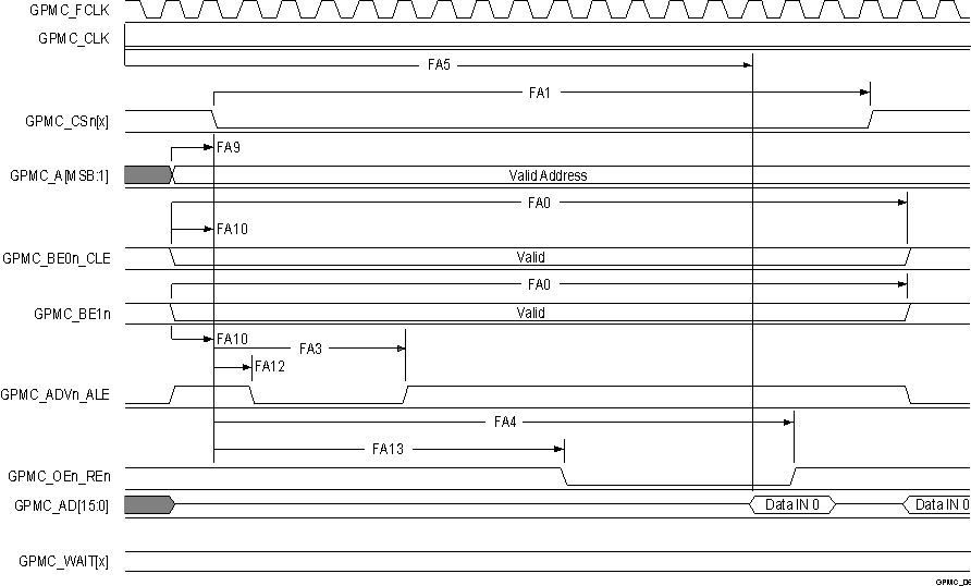
A. In GPMC_CSn[x], x is equal to 0,
1, 2 or 3. In GPMC_WAIT[x], x is equal to 0 or 1.
B. FA5 parameter illustrates amount
of time required to internally sample input data. It is expressed in number of
GPMC functional clock cycles. From start of read cycle and after FA5 functional
clock cycles, input data will be internally sampled by active functional clock
edge. FA5 value must be stored inside AccessTime register bits field.
C. GPMC_FCLK is an internal clock
(GPMC functional clock) not provided externally.
Figure 6-53 GPMC and
NOR Flash—Asynchronous Read—Single Word 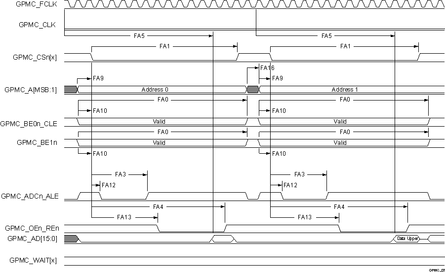
A. In GPMC_CSn[x], x is equal to 0,
1, 2 or 3. In GPMC_WAIT[x], x is equal to 0 or 1.
B. FA5 parameter illustrates amount
of time required to internally sample input data. It is expressed in number of
GPMC functional clock cycles. From start of read cycle and after FA5 functional
clock cycles, input data will be internally sampled by active functional clock
edge. FA5 value must be stored inside AccessTime register bits field.
C. GPMC_FCLK is an internal clock
(GPMC functional clock) not provided externally.
Figure 6-54 GPMC and
NOR Flash—Asynchronous Read—32-Bit 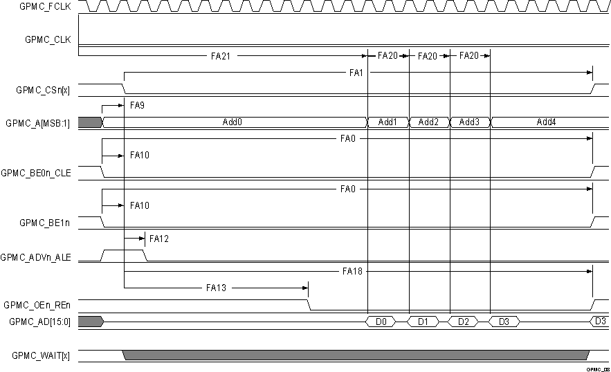
A. In GPMC_CSn[x], x is equal to 0,
1, 2 or 3. In GPMC_WAIT[x], x is equal to 0 or 1.
B. FA21 parameter illustrates
amount of time required to internally sample first input page data. It is
expressed in number of GPMC functional clock cycles. From start of read cycle
and after FA21 functional clock cycles, first input page data will be internally
sampled by active functional clock edge. FA21 calculation must be stored inside
AccessTime register bits field.
C. FA20 parameter illustrates
amount of time required to internally sample successive input page data. It is
expressed in number of GPMC functional clock cycles. After each access to input
page data, next input page data will be internally sampled by active functional
clock edge after FA20 functional clock cycles. FA20 is also the duration of
address phases for successive input page data (excluding first input page data).
FA20 value must be stored in PageBurstAccessTime register bits field.
D. GPMC_FCLK is an internal clock
(GPMC functional clock) not provided externally.
Figure 6-55 GPMC and
NOR Flash—Asynchronous Read—Page Mode 4x16-Bit 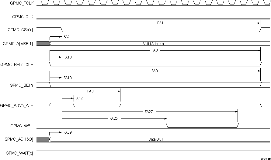
A. In GPMC_CSn[x], x is equal to 0,
1, 2 or 3. In GPMC_WAIT[x], x is equal to 0 or 1.
Figure 6-56 GPMC and
NOR Flash—Asynchronous Write—Single Word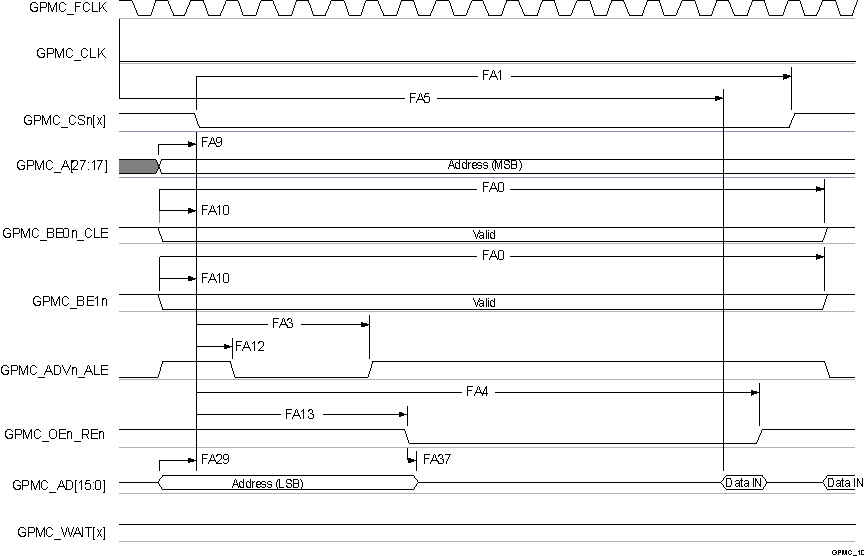
A. In GPMC_CSn[x], x is equal to 0,
1, 2 or 3. In GPMC_WAIT[x], x is equal to 0 or 1.
B. FA5 parameter illustrates amount
of time required to internally sample input data. It is expressed in number of
GPMC functional clock cycles. From start of read cycle and after FA5 functional
clock cycles, input data will be internally sampled by active functional clock
edge. FA5 value must be stored inside AccessTime register bits field.
C. GPMC_FCLK is an internal clock
(GPMC functional clock) not provided externally.
Figure 6-57 GPMC and
Multiplexed NOR Flash—Asynchronous Read—Single Word 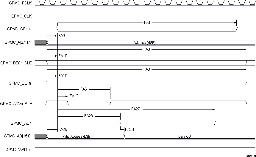
A. In GPMC_CSn[x], x is equal to 0,
1, 2 or 3. In GPMC_WAIT[x], x is equal to 0 or 1.
Figure 6-58 GPMC and
Multiplexed NOR Flash—Asynchronous Write—Single Word