ZHCSLA7C December 2019 – September 2023 AM6526 , AM6528 , AM6546 , AM6548
PRODUCTION DATA
- 1
- 1 特性
- 2 应用
- 3 说明
- 4 Device Comparison
-
5 Terminal Configuration and Functions
- 5.1 Pin Diagram
- 5.2 Pin Attributes
- 5.3
Signal Descriptions
- 5.3.1 ADC
- 5.3.2 CAL
- 5.3.3 CPSW2G
- 5.3.4 DDRSS
- 5.3.5 DMTIMER
- 5.3.6 DSS
- 5.3.7 ECAP
- 5.3.8 EHRPWM
- 5.3.9 EQEP
- 5.3.10 GPIO
- 5.3.11 GPMC
- 5.3.12 HyperBus
- 5.3.13 I2C
- 5.3.14 MCAN
- 5.3.15 MCASP
- 5.3.16 MCSPI
- 5.3.17 MMCSD
- 5.3.18 CPTS
- 5.3.19 OLDI
- 5.3.20 OSPI
- 5.3.21 PRU_ICSSG
- 5.3.22 SERDES
- 5.3.23 UART
- 5.3.24 USB
- 5.3.25 Emulation and Debug
- 5.3.26 System and Miscellaneous
- 5.3.27 Power Supply
- 5.4 Pin Multiplexing
- 5.5 Connections for Unused Pins
-
6 Specifications
- 6.1 Absolute Maximum Ratings
- 6.2 ESD Ratings
- 6.3 Power-On Hours (POH)
- 6.4 Recommended Operating Conditions
- 6.5 Operating Performance Points
- 6.6
Electrical Characteristics
- 6.6.1 I2C OPEN DRAIN DC Electrical Characteristics
- 6.6.2 Analog OSC Buffers DC Electrical Characteristics
- 6.6.3 Analog ADC DC Electrical Characteristics
- 6.6.4 DPHY CSI2 Buffers DC Electrical Characteristics
- 6.6.5 OLDI LVDS Buffers DC Electrical Characteristics
- 6.6.6 USBHS Buffers DC Electrical Characteristics
- 6.6.7 SERDES Buffers DC Electrical Characteristics
- 6.7 VPP Specifications for One-Time Programmable (OTP) eFuses
- 6.8 Thermal Resistance Characteristics
- 6.9
Timing and Switching Characteristics
- 6.9.1 Timing Parameters and Information
- 6.9.2 Power Supply Sequencing
- 6.9.3 System Timing
- 6.9.4
Clock Specifications
- 6.9.4.1
Input Clocks / Oscillators
- 6.9.4.1.1 WKUP_OSC0 Internal Oscillator Clock Source
- 6.9.4.1.2 WKUP_OSC0 LVCMOS Digital Clock Source
- 6.9.4.1.3 Auxiliary OSC1 Internal Oscillator Clock Source
- 6.9.4.1.4 Auxiliary OSC1 LVCMOS Digital Clock Source
- 6.9.4.1.5 Auxiliary OSC1 Not Used
- 6.9.4.1.6 WKUP_LFOSC0 Internal Oscillator Clock Source
- 6.9.4.1.7 WKUP_LFOSC0 LVCMOS Digital Clock Source
- 6.9.4.1.8 WKUP_LFOSC0 Not Used
- 6.9.4.2 Output Clocks
- 6.9.4.3 PLLs
- 6.9.4.4 Recommended Clock and Control Signal Transition Behavior
- 6.9.4.5 Module and Peripheral Clock Frequencies
- 6.9.4.1
Input Clocks / Oscillators
- 6.9.5
Peripherals
- 6.9.5.1 VIN
- 6.9.5.2
CPSW2G
- 6.9.5.2.1 CPSW2G MDIO Interface Timings
- 6.9.5.2.2 CPSW2G RMII Timings
- 6.9.5.2.3
CPSW2G RGMII Timings
- 6.9.5.2.3.1 Timing Requirements for RGMII[x]_RCLK - RGMII Mode
- 6.9.5.2.3.2 Timing Requirements for RGMII[x]_RD[3:0], and RGMII[x]_RCTL - RGMII Mode
- 6.9.5.2.3.3 Switching Characteristics for RGMII[x]_TCLK - RGMII Mode
- 6.9.5.2.3.4 Switching Characteristics for RGMII[x]_TD[3:0], and RGMII[x]_TX_CTL - RGMII Mode
- 6.9.5.3 CSI2
- 6.9.5.4 DDRSS
- 6.9.5.5 DSS
- 6.9.5.6 eCAP
- 6.9.5.7 ePWM
- 6.9.5.8 eQEP
- 6.9.5.9 GPIO
- 6.9.5.10 GPMC
- 6.9.5.11 HyperBus
- 6.9.5.12 I2C
- 6.9.5.13 MCAN
- 6.9.5.14 MCASP
- 6.9.5.15 MCSPI
- 6.9.5.16 MMCSD
- 6.9.5.17 CPTS
- 6.9.5.18 OSPI
- 6.9.5.19 OLDI
- 6.9.5.20 PCIE
- 6.9.5.21
PRU_ICSSG
- 6.9.5.21.1
Programmable Real-Time Unit (PRU_ICSSG PRU)
- 6.9.5.21.1.1 PRU_ICSSG PRU Direct Input/Output Mode Electrical Data and Timing
- 6.9.5.21.1.2 PRU_ICSSG PRU Parallel Capture Mode Electrical Data and Timing
- 6.9.5.21.1.3 PRU_ICSSG PRU Shift Mode Electrical Data and Timing
- 6.9.5.21.1.4 PRU_ICSSG PRU Sigma Delta and Peripheral Interface Modes Electrical Data and Timing
- 6.9.5.21.2 PRU_ICSSG Pulse Width Modulation (PWM)
- 6.9.5.21.3 PRU_ICSSG Industrial Ethernet Peripheral (PRU_ICSSG IEP)
- 6.9.5.21.4 PRU_ICSSG Universal Asynchronous Receiver Transmitter (PRU-ICSS UART)
- 6.9.5.21.5 PRU_ICSSG Enhanced Capture Peripheral (PRU-ICSS ECAP)
- 6.9.5.21.6
PRU_ICSSG RGMII, MII_RT, and Switch
- 6.9.5.21.6.1 PRU_ICSSG MDIO Electrical Data and Timing
- 6.9.5.21.6.2
PRU_ICSSG RGMII Electrical Data and Timing
- 6.9.5.21.6.2.1 PRU_ICSSG RGMII Timing Requirements - RGMII_RXC
- 6.9.5.21.6.2.2 PRU_ICSSG RGMII Timing Requirements - RGMII_RD[3:0] and RGMII_RX_CTL
- 6.9.5.21.6.2.3 PRU_ICSSG RGMII Switching Characteristics - RGMII_TXC
- 6.9.5.21.6.2.4 PRU_ICSSG RGMII Switching Characteristics - RGMII_TD[3:0] and RGMII_TX_CTL
- 6.9.5.21.6.3
PRU_ICSSG MII_RT Electrical Data and Timing
- 6.9.5.21.6.3.1 PRU_ICSSG MII_RT Timing Requirements – MII_RX_CLK
- 6.9.5.21.6.3.2 PRU_ICSSG MII_RT Timing Requirements – MII_RXD[3:0], MII_RX_DV, and MII_RX_ER
- 6.9.5.21.6.3.3 PRU_ICSSG MII_RT Switching Characteristics – MII_TX_CLK
- 6.9.5.21.6.3.4 PRU_ICSSG MII_RT Switching Characteristics – MII_TXD[3:0] and MII_TXEN
- 6.9.5.21.1
Programmable Real-Time Unit (PRU_ICSSG PRU)
- 6.9.5.22 Timers
- 6.9.5.23 UART
- 6.9.5.24 USB
- 6.9.5.25 Emulation and Debug
-
7 Detailed Description
- 7.1 Overview
- 7.2 Processor Subsystems
- 7.3 Accelerators and Coprocessors
- 7.4
Other Subsystems
- 7.4.1 DMSC
- 7.4.2 MSMC
- 7.4.3 NAVSS
- 7.4.4 PDMA Controller
- 7.4.5
Peripherals
- 7.4.5.1 ADC
- 7.4.5.2 CAL
- 7.4.5.3 CPSW2G
- 7.4.5.4 DCC
- 7.4.5.5 DDRSS
- 7.4.5.6 DSS
- 7.4.5.7 ЕCAP
- 7.4.5.8 EPWM
- 7.4.5.9 ELM
- 7.4.5.10 ESM
- 7.4.5.11 EQEP
- 7.4.5.12 GPIO
- 7.4.5.13 GPMC
- 7.4.5.14 HyperBus
- 7.4.5.15 I2C
- 7.4.5.16 MCAN
- 7.4.5.17 MCASP
- 7.4.5.18 MCRC
- 7.4.5.19 MCSPI
- 7.4.5.20 MMCSD
- 7.4.5.21 OSPI
- 7.4.5.22 PCIE
- 7.4.5.23 SerDes
- 7.4.5.24 RTI
- 7.4.5.25 Timers
- 7.4.5.26 UART
- 7.4.5.27 USB
- 7.5 Identification
- 7.6 Boot Modes
-
8 Applications, Implementation, and Layout
- 8.1 Device Connection and Layout Fundamentals
- 8.2
Peripheral- and Interface-Specific Design Information
- 8.2.1 DDR Board Design and Layout Guidelines
- 8.2.2 OSPI Board Design and Layout Guidelines
- 8.2.3 USB Design Guidelines
- 8.2.4 High Speed Differential Signal Routing Guidance
- 8.2.5 System Power Supply Monitor Design Guidelines
- 8.2.6 MMC Design Guidelines
- 8.2.7 Integrated Power Management Features
- 8.2.8 External Capacitors
- 8.2.9 Thermal Solution Guidance
- 9 Device and Documentation Support
- 10Revision History
- 11Mechanical, Packaging, and Orderable Information
8.2.8.1 LVCMOS External Capacitor Connections
Each VDDSHV[8:0], and VDDSHV[2:0]_WKUP can be configured as 1.8 V or 3.3 V. Figure 8-7 through Figure 8-10 illustrate different system configurations for the dual-voltage I/O supplies.
VDDSHV[8:0], and VDDSHV[2:0]_WKUP are the dual-voltage LVCMOS I/O supplies, while VDDS[8:0] are the dual-voltage LVCMOS I/O bias supplies. If any of the VDDSHV[8:0] or VDDSHV[2:0]_WKUP are configured for 3.3 V operation, the corresponding VDDS[8:0] or VDDS[2:0]_WKUP should be sourced from the internal I/O Bias LDO. When any of the VDDSHV[8:0] or VDDSHV[2:0]_WKUP are configured for 1.8 V operation, both VDDS[8:0] and VDDSHV[8:0] or VDDS[2:0]_WKUP and VDDSHV[2:0]_WKUP should be supplied from the same source.
Two I/O Bias LDOs are integrated on this device to share load current. The recommended load sharing is as follows:
- IOLDO0 : VDDS0, VDDS1, VDDS2, VDDS5, VDDS7, VDDS8
- IOLDO1 : VDDS3, VDDS4, VDDS6
Figure 8-7 shows all VDDSHV[8:0], and VDDSHV[2:0]_WKUP supplies configured for 3.3V operation.
![AM6548 AM6528 AM6546 AM6526 All VDDSHV[8:0], and VDDSHV[2:0]_WKUP Supplies Configured for 3.3 V
Operation GUID-ECF0EAE1-E9E6-4267-B087-D16B4675BA1A-low.gif](/ods/images/ZHCSLA7C/GUID-ECF0EAE1-E9E6-4267-B087-D16B4675BA1A-low.gif) Figure 8-7 All VDDSHV[8:0], and VDDSHV[2:0]_WKUP Supplies Configured for 3.3 V
Operation
Figure 8-7 All VDDSHV[8:0], and VDDSHV[2:0]_WKUP Supplies Configured for 3.3 V
OperationFigure 8-8 shows all VDDSHV[8:0] and VDDSHV[2:0]_WKUP supplies configured for 1.8 V operation.
![AM6548 AM6528 AM6546 AM6526 All VDDSHV[8:0] and
VDDSHV[2:0]_WKUP Supplies Configured for 1.8V Operation GUID-7214D0F2-DCD8-4A4E-9F3E-6329A7571880-low.gif](/ods/images/ZHCSLA7C/GUID-7214D0F2-DCD8-4A4E-9F3E-6329A7571880-low.gif) Figure 8-8 All VDDSHV[8:0] and
VDDSHV[2:0]_WKUP Supplies Configured for 1.8V Operation
Figure 8-8 All VDDSHV[8:0] and
VDDSHV[2:0]_WKUP Supplies Configured for 1.8V OperationFigure 8-9 shows a split configuration where VDDSHV[0, 1, 2, 5, 8] and VDDSHV0_WKUP are configured for 3.3 V operation, while VDDSHV[3, 4, 6, 7] and VDDSHV[2:1]_WKUP are configured for 1.8 V operation. Note the colors indicate rails that are tied to the same source.
![AM6548 AM6528 AM6546 AM6526 VDDSHV[8:0] and
VDDSHV[2:0]_WKUP Supplies Configured for Combination of 1.8 V or 3.3 V
Operation GUID-6F426FC1-5394-48BC-A35B-42867875CC06-low.gif](/ods/images/ZHCSLA7C/GUID-6F426FC1-5394-48BC-A35B-42867875CC06-low.gif) Figure 8-9 VDDSHV[8:0] and
VDDSHV[2:0]_WKUP Supplies Configured for Combination of 1.8 V or 3.3 V
Operation
Figure 8-9 VDDSHV[8:0] and
VDDSHV[2:0]_WKUP Supplies Configured for Combination of 1.8 V or 3.3 V
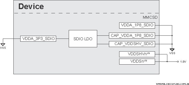
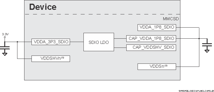
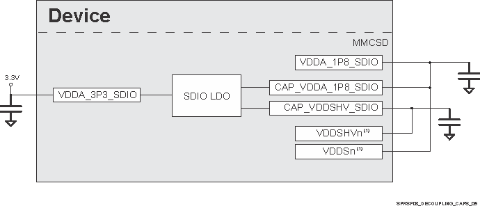
OperationFigure 8-10through Figure 8-12 illustrates the system configuration when VDDSHV6 or VDDSHV7 is used as the MMCSD supply.
 Figure 8-10 VDDSHV6 or VDDSHV7 Used as the
MMCSD Supply for Fixed 1.8V IO
 Figure 8-11 VDDSHV6 or VDDSHV7 Used as the
MMCSD Supply for Fixed 3.3V IO
 Figure 8-12 VDDSHV6 or VDDSHV7 Used as the
MMCSD Supply for Dynamic 3.3V/1.8V IO