ZHCSLA7C December 2019 – September 2023 AM6526 , AM6528 , AM6546 , AM6548
PRODUCTION DATA
- 1
- 1 特性
- 2 应用
- 3 说明
- 4 Device Comparison
-
5 Terminal Configuration and Functions
- 5.1 Pin Diagram
- 5.2 Pin Attributes
- 5.3
Signal Descriptions
- 5.3.1 ADC
- 5.3.2 CAL
- 5.3.3 CPSW2G
- 5.3.4 DDRSS
- 5.3.5 DMTIMER
- 5.3.6 DSS
- 5.3.7 ECAP
- 5.3.8 EHRPWM
- 5.3.9 EQEP
- 5.3.10 GPIO
- 5.3.11 GPMC
- 5.3.12 HyperBus
- 5.3.13 I2C
- 5.3.14 MCAN
- 5.3.15 MCASP
- 5.3.16 MCSPI
- 5.3.17 MMCSD
- 5.3.18 CPTS
- 5.3.19 OLDI
- 5.3.20 OSPI
- 5.3.21 PRU_ICSSG
- 5.3.22 SERDES
- 5.3.23 UART
- 5.3.24 USB
- 5.3.25 Emulation and Debug
- 5.3.26 System and Miscellaneous
- 5.3.27 Power Supply
- 5.4 Pin Multiplexing
- 5.5 Connections for Unused Pins
-
6 Specifications
- 6.1 Absolute Maximum Ratings
- 6.2 ESD Ratings
- 6.3 Power-On Hours (POH)
- 6.4 Recommended Operating Conditions
- 6.5 Operating Performance Points
- 6.6
Electrical Characteristics
- 6.6.1 I2C OPEN DRAIN DC Electrical Characteristics
- 6.6.2 Analog OSC Buffers DC Electrical Characteristics
- 6.6.3 Analog ADC DC Electrical Characteristics
- 6.6.4 DPHY CSI2 Buffers DC Electrical Characteristics
- 6.6.5 OLDI LVDS Buffers DC Electrical Characteristics
- 6.6.6 USBHS Buffers DC Electrical Characteristics
- 6.6.7 SERDES Buffers DC Electrical Characteristics
- 6.7 VPP Specifications for One-Time Programmable (OTP) eFuses
- 6.8 Thermal Resistance Characteristics
- 6.9
Timing and Switching Characteristics
- 6.9.1 Timing Parameters and Information
- 6.9.2 Power Supply Sequencing
- 6.9.3 System Timing
- 6.9.4
Clock Specifications
- 6.9.4.1
Input Clocks / Oscillators
- 6.9.4.1.1 WKUP_OSC0 Internal Oscillator Clock Source
- 6.9.4.1.2 WKUP_OSC0 LVCMOS Digital Clock Source
- 6.9.4.1.3 Auxiliary OSC1 Internal Oscillator Clock Source
- 6.9.4.1.4 Auxiliary OSC1 LVCMOS Digital Clock Source
- 6.9.4.1.5 Auxiliary OSC1 Not Used
- 6.9.4.1.6 WKUP_LFOSC0 Internal Oscillator Clock Source
- 6.9.4.1.7 WKUP_LFOSC0 LVCMOS Digital Clock Source
- 6.9.4.1.8 WKUP_LFOSC0 Not Used
- 6.9.4.2 Output Clocks
- 6.9.4.3 PLLs
- 6.9.4.4 Recommended Clock and Control Signal Transition Behavior
- 6.9.4.5 Module and Peripheral Clock Frequencies
- 6.9.4.1
Input Clocks / Oscillators
- 6.9.5
Peripherals
- 6.9.5.1 VIN
- 6.9.5.2
CPSW2G
- 6.9.5.2.1 CPSW2G MDIO Interface Timings
- 6.9.5.2.2 CPSW2G RMII Timings
- 6.9.5.2.3
CPSW2G RGMII Timings
- 6.9.5.2.3.1 Timing Requirements for RGMII[x]_RCLK - RGMII Mode
- 6.9.5.2.3.2 Timing Requirements for RGMII[x]_RD[3:0], and RGMII[x]_RCTL - RGMII Mode
- 6.9.5.2.3.3 Switching Characteristics for RGMII[x]_TCLK - RGMII Mode
- 6.9.5.2.3.4 Switching Characteristics for RGMII[x]_TD[3:0], and RGMII[x]_TX_CTL - RGMII Mode
- 6.9.5.3 CSI2
- 6.9.5.4 DDRSS
- 6.9.5.5 DSS
- 6.9.5.6 eCAP
- 6.9.5.7 ePWM
- 6.9.5.8 eQEP
- 6.9.5.9 GPIO
- 6.9.5.10 GPMC
- 6.9.5.11 HyperBus
- 6.9.5.12 I2C
- 6.9.5.13 MCAN
- 6.9.5.14 MCASP
- 6.9.5.15 MCSPI
- 6.9.5.16 MMCSD
- 6.9.5.17 CPTS
- 6.9.5.18 OSPI
- 6.9.5.19 OLDI
- 6.9.5.20 PCIE
- 6.9.5.21
PRU_ICSSG
- 6.9.5.21.1
Programmable Real-Time Unit (PRU_ICSSG PRU)
- 6.9.5.21.1.1 PRU_ICSSG PRU Direct Input/Output Mode Electrical Data and Timing
- 6.9.5.21.1.2 PRU_ICSSG PRU Parallel Capture Mode Electrical Data and Timing
- 6.9.5.21.1.3 PRU_ICSSG PRU Shift Mode Electrical Data and Timing
- 6.9.5.21.1.4 PRU_ICSSG PRU Sigma Delta and Peripheral Interface Modes Electrical Data and Timing
- 6.9.5.21.2 PRU_ICSSG Pulse Width Modulation (PWM)
- 6.9.5.21.3 PRU_ICSSG Industrial Ethernet Peripheral (PRU_ICSSG IEP)
- 6.9.5.21.4 PRU_ICSSG Universal Asynchronous Receiver Transmitter (PRU-ICSS UART)
- 6.9.5.21.5 PRU_ICSSG Enhanced Capture Peripheral (PRU-ICSS ECAP)
- 6.9.5.21.6
PRU_ICSSG RGMII, MII_RT, and Switch
- 6.9.5.21.6.1 PRU_ICSSG MDIO Electrical Data and Timing
- 6.9.5.21.6.2
PRU_ICSSG RGMII Electrical Data and Timing
- 6.9.5.21.6.2.1 PRU_ICSSG RGMII Timing Requirements - RGMII_RXC
- 6.9.5.21.6.2.2 PRU_ICSSG RGMII Timing Requirements - RGMII_RD[3:0] and RGMII_RX_CTL
- 6.9.5.21.6.2.3 PRU_ICSSG RGMII Switching Characteristics - RGMII_TXC
- 6.9.5.21.6.2.4 PRU_ICSSG RGMII Switching Characteristics - RGMII_TD[3:0] and RGMII_TX_CTL
- 6.9.5.21.6.3
PRU_ICSSG MII_RT Electrical Data and Timing
- 6.9.5.21.6.3.1 PRU_ICSSG MII_RT Timing Requirements – MII_RX_CLK
- 6.9.5.21.6.3.2 PRU_ICSSG MII_RT Timing Requirements – MII_RXD[3:0], MII_RX_DV, and MII_RX_ER
- 6.9.5.21.6.3.3 PRU_ICSSG MII_RT Switching Characteristics – MII_TX_CLK
- 6.9.5.21.6.3.4 PRU_ICSSG MII_RT Switching Characteristics – MII_TXD[3:0] and MII_TXEN
- 6.9.5.21.1
Programmable Real-Time Unit (PRU_ICSSG PRU)
- 6.9.5.22 Timers
- 6.9.5.23 UART
- 6.9.5.24 USB
- 6.9.5.25 Emulation and Debug
-
7 Detailed Description
- 7.1 Overview
- 7.2 Processor Subsystems
- 7.3 Accelerators and Coprocessors
- 7.4
Other Subsystems
- 7.4.1 DMSC
- 7.4.2 MSMC
- 7.4.3 NAVSS
- 7.4.4 PDMA Controller
- 7.4.5
Peripherals
- 7.4.5.1 ADC
- 7.4.5.2 CAL
- 7.4.5.3 CPSW2G
- 7.4.5.4 DCC
- 7.4.5.5 DDRSS
- 7.4.5.6 DSS
- 7.4.5.7 ЕCAP
- 7.4.5.8 EPWM
- 7.4.5.9 ELM
- 7.4.5.10 ESM
- 7.4.5.11 EQEP
- 7.4.5.12 GPIO
- 7.4.5.13 GPMC
- 7.4.5.14 HyperBus
- 7.4.5.15 I2C
- 7.4.5.16 MCAN
- 7.4.5.17 MCASP
- 7.4.5.18 MCRC
- 7.4.5.19 MCSPI
- 7.4.5.20 MMCSD
- 7.4.5.21 OSPI
- 7.4.5.22 PCIE
- 7.4.5.23 SerDes
- 7.4.5.24 RTI
- 7.4.5.25 Timers
- 7.4.5.26 UART
- 7.4.5.27 USB
- 7.5 Identification
- 7.6 Boot Modes
-
8 Applications, Implementation, and Layout
- 8.1 Device Connection and Layout Fundamentals
- 8.2
Peripheral- and Interface-Specific Design Information
- 8.2.1 DDR Board Design and Layout Guidelines
- 8.2.2 OSPI Board Design and Layout Guidelines
- 8.2.3 USB Design Guidelines
- 8.2.4 High Speed Differential Signal Routing Guidance
- 8.2.5 System Power Supply Monitor Design Guidelines
- 8.2.6 MMC Design Guidelines
- 8.2.7 Integrated Power Management Features
- 8.2.8 External Capacitors
- 8.2.9 Thermal Solution Guidance
- 9 Device and Documentation Support
- 10Revision History
- 11Mechanical, Packaging, and Orderable Information
6.9.5.10.1.2 GPMC and NOR Flash Switching Characteristics—Synchronous Mode
| NO.(2) | PARAMETER | DESCRIPTION | MODE(19) | MIN | MAX | UNIT |
|---|---|---|---|---|---|---|
| F0 | tc(clk) | Period, output clock GPMC_CLK (18) | div_by_1_mode; GPMC_FCLK_MUX_100; TIMEPARAGRANULARITY_X1 | 10 | ns | |
| F1 | tw(clkH) | Typical pulse duration, output clock GPMC_CLK high | div_by_1_mode; GPMC_FCLK_MUX_100; TIMEPARAGRANULARITY_X1 | -0.3+0.475*P (15) | ns | |
| F1 | tw(clkL) | Typical pulse duration, output clock GPMC_CLK low | div_by_1_mode; GPMC_FCLK_MUX_100; TIMEPARAGRANULARITY_X1 | -0.3+0.475*P (15) | ns | |
| F2 | td(clkH-csnV) | Delay time, output clock GPMC_CLK rising edge to output chip select GPMC_CSn[x] transition (14) | div_by_1_mode; GPMC_FCLK_MUX_100; TIMEPARAGRANULARITY_X1; no extra_delay | -2.2+F (6) | 4.5+F (6) | ns |
| F3 | td(clkH-csnIV) | Delay time, output clock GPMC_CLK rising edge to output chip select GPMC_CSn[x] invalid (14) | div_by_1_mode; GPMC_FCLK_MUX_100; TIMEPARAGRANULARITY_X1; no extra_delay | -2.2+E (5) | 4.5+E (5) | ns |
| F4 | td(aV-clk) | Delay time, output address GPMC_A[27:1] valid to output clock GPMC_CLK first edge | div_by_1_mode; GPMC_FCLK_MUX_100; TIMEPARAGRANULARITY_X1 | -2.3+B (2) | 4.5+B (2) | ns |
| F5 | td(clkH-aIV) | Delay time, output clock GPMC_CLK rising edge to output address GPMC_A[27:1] invalid | div_by_1_mode; GPMC_FCLK_MUX_100; TIMEPARAGRANULARITY_X1 | -2.3 | 4.5 | ns |
| F6 | td(be[x]nV-clk) | Delay time, output lower byte enable and command latch enable GPMC_BE0n_CLE, output upper byte enable GPMC_BE1n valid to output clock GPMC_CLK first edge | div_by_1_mode; GPMC_FCLK_MUX_100; TIMEPARAGRANULARITY_X1 | -2.3+B (2) | 1.9+B (2) | ns |
| F7 | td(clkH-be[x]nIV) | Delay time, output clock GPMC_CLK rising edge to output lower byte enable and command latch enable GPMC_BE0n_CLE, output upper byte enable GPMC_BE1n invalid (11) | div_by_1_mode; GPMC_FCLK_MUX_100; TIMEPARAGRANULARITY_X1 | -2.3+D (4) | 1.9+D (4) | ns |
| F7 | td(clkL-be[x]nIV) | Delay time, GPMC_CLK falling edge to GPMC_BE0n_CLE, GPMC_BE1n invalid (12) | div_by_1_mode; GPMC_FCLK_MUX_100; TIMEPARAGRANULARITY_X1 | -2.3+D (4) | 1.9+D (4) | ns |
| F7 | td(clkL-be[x]nIV). | Delay time, GPMC_CLK falling edge to GPMC_BE0n_CLE, GPMC_BE1n invalid (13) | div_by_1_mode; GPMC_FCLK_MUX_100; TIMEPARAGRANULARITY_X1 | -2.3+D (4) | 1.9+D (4) | ns |
| F8 | td(clkH-advn) | Delay time, output clock GPMC_CLK rising edge to output address valid and address latch enable GPMC_ADVn_ALE transition | div_by_1_mode; GPMC_FCLK_MUX_100; TIMEPARAGRANULARITY_X1; no extra_delay | -2.3+G (7) | 4.5+G (7) | ns |
| F9 | td(clkH-advnIV) | Delay time, output clock GPMC_CLK rising edge to output address valid and address latch enable GPMC_ADVn_ALE invalid | div_by_1_mode; GPMC_FCLK_MUX_100; TIMEPARAGRANULARITY_X1; no extra_delay | -2.3+D (4) | 4.5+D (4) | ns |
| F10 | td(clkH-oen) | Delay time, output clock GPMC_CLK rising edge to output enable GPMC_OEn_REn transition | div_by_1_mode; GPMC_FCLK_MUX_100; TIMEPARAGRANULARITY_X1; no extra_delay | -2.3H (8) | 3.5+H (8) | ns |
| F11 | td(clkH-oenIV) | Delay time, output clock GPMC_CLK rising edge to output enable GPMC_OEn_REn invalid | div_by_1_mode; GPMC_FCLK_MUX_100; TIMEPARAGRANULARITY_X1; no extra_delay | -2.3+E (8) | 3.5+E (8) | ns |
| F14 | td(clkH-wen) | Delay time, output clock GPMC_CLK rising edge to output write enable GPMC_WEn transition | div_by_1_mode; GPMC_FCLK_MUX_100; TIMEPARAGRANULARITY_X1; no extra_delay | -2.3+I (9) | 4.5+I (9) | ns |
| F15 | td(clkH-do) | Delay time, output clock GPMC_CLK rising edge to output data GPMC_AD[15:0] transition (11) | div_by_1_mode; GPMC_FCLK_MUX_100; TIMEPARAGRANULARITY_X1 | -2.3+J (10) | 2.7+J (10) | ns |
| F15 | td(clkL-do) | Delay time, GPMC_CLK falling edge to GPMC_AD[15:0] data bus transition (12) | div_by_1_mode; GPMC_FCLK_MUX_100; TIMEPARAGRANULARITY_X1 | -2.3+J (10) | 2.7+J (10) | ns |
| F15 | td(clkL-do). | Delay time, GPMC_CLK falling edge to GPMC_AD[15:0] data bus transition (13) | div_by_1_mode; GPMC_FCLK_MUX_100; TIMEPARAGRANULARITY_X1 | -2.3+J (10) | 2.7+J (10) | ns |
| F17 | td(clkH-be[x]n) | Delay time, output clock GPMC_CLK rising edge to output lower byte enable and command latch enable GPMC_BE0n_CLE transition (11) | div_by_1_mode; GPMC_FCLK_MUX_100; TIMEPARAGRANULARITY_X1 | -2.3+J (10) | 1.9+J (10) | ns |
| F17 | td(clkL-be[x]n) | Delay time, GPMC_CLK falling edge to GPMC_BE0n_CLE, GPMC_BE1n transition (12) | div_by_1_mode; GPMC_FCLK_MUX_100; TIMEPARAGRANULARITY_X1 | -2.3+J (10) | 1.9+J (10) | ns |
| F17 | td(clkL-be[x]n). | Delay time, GPMC_CLK falling edge to GPMC_BE0n_CLE, GPMC_BE1n transition (13) | div_by_1_mode; GPMC_FCLK_MUX_100; TIMEPARAGRANULARITY_X1 | -2.3+J (10) | 1.9+J (10) | ns |
| F18 | tw(csnV) | Pulse duration, output chip select GPMC_CSn[x] low (14) | Read | 0+A (1) | ns | |
| Write | 0+A (1) | ns | ||||
| F19 | tw(be[x]nV) | Pulse duration, output lower byte enable and command latch enable GPMC_BE0n_CLE, output upper byte enable GPMC_BE1n low | Read | 0+C (3) | ns | |
| Write | 0+C (3) | ns | ||||
| F20 | tw(advnV) | Pulse duration, output address valid and address latch enable GPMC_ADVn_ALE low | Read | 0+K (16) | ns | |
| Write | 0+K (16) | ns |
(1) For single read: A = (CSRdOffTime - CSOnTime) × (TimeParaGranularity + 1) × GPMC_FCLK(17)
For burst read: A = (CSRdOffTime - CSOnTime + (n - 1) × PageBurstAccessTime) × (TimeParaGranularity + 1) × GPMC_FCLK(17)
For burst write: A = (CSWrOffTime - CSOnTime + (n - 1) × PageBurstAccessTime) × (TimeParaGranularity + 1) × GPMC_FCLK(17)
With n being the page burst access number.
For burst read: A = (CSRdOffTime - CSOnTime + (n - 1) × PageBurstAccessTime) × (TimeParaGranularity + 1) × GPMC_FCLK(17)
For burst write: A = (CSWrOffTime - CSOnTime + (n - 1) × PageBurstAccessTime) × (TimeParaGranularity + 1) × GPMC_FCLK(17)
With n being the page burst access number.
(2) B = ClkActivationTime × GPMC_FCLK(17)
(3) For single read: C = RdCycleTime × (TimeParaGranularity + 1) × GPMC_FCLK(17)
For burst read: C = (RdCycleTime + (n - 1) × PageBurstAccessTime) × (TimeParaGranularity + 1) × GPMC_FCLK(17)
For burst write: C = (WrCycleTime + (n - 1) × PageBurstAccessTime) × (TimeParaGranularity + 1) × GPMC_FCLK(17)
With n being the page burst access number.
For burst read: C = (RdCycleTime + (n - 1) × PageBurstAccessTime) × (TimeParaGranularity + 1) × GPMC_FCLK(17)
For burst write: C = (WrCycleTime + (n - 1) × PageBurstAccessTime) × (TimeParaGranularity + 1) × GPMC_FCLK(17)
With n being the page burst access number.
(4) For single read: D = (RdCycleTime - AccessTime) × (TimeParaGranularity + 1) × GPMC_FCLK(17)
For burst read: D = (RdCycleTime - AccessTime) × (TimeParaGranularity + 1) × GPMC_FCLK(17)
For burst write: D = (WrCycleTime - AccessTime) × (TimeParaGranularity + 1) × GPMC_FCLK(17)
For burst read: D = (RdCycleTime - AccessTime) × (TimeParaGranularity + 1) × GPMC_FCLK(17)
For burst write: D = (WrCycleTime - AccessTime) × (TimeParaGranularity + 1) × GPMC_FCLK(17)
(5) For single read: E = (CSRdOffTime - AccessTime) × (TimeParaGranularity + 1) × GPMC_FCLK(17)
For burst read: E = (CSRdOffTime - AccessTime) × (TimeParaGranularity + 1) × GPMC_FCLK(17)
For burst write: E = (CSWrOffTime - AccessTime) × (TimeParaGranularity + 1) × GPMC_FCLK(17)
For burst read: E = (CSRdOffTime - AccessTime) × (TimeParaGranularity + 1) × GPMC_FCLK(17)
For burst write: E = (CSWrOffTime - AccessTime) × (TimeParaGranularity + 1) × GPMC_FCLK(17)
(6) For csn falling edge (CS activated):
- Case GpmcFCLKDivider = 0:
- F = 0.5 × CSExtraDelay × GPMC_FCLK(17)
- Case GpmcFCLKDivider = 1:
- Case GpmcFCLKDivider = 2:
(7) For ADV falling edge (ADV activated):
For ADV rising edge (ADV deactivated) in Reading mode:
For ADV rising edge (ADV deactivated) in Writing mode:
- Case GpmcFCLKDivider = 0:
- G = 0.5 × ADVExtraDelay × GPMC_FCLK(17)
- Case GpmcFCLKDivider = 1:
- Case GpmcFCLKDivider = 2:
- G = 0.5 × ADVExtraDelay × GPMC_FCLK(17) if ((ADVOnTime - ClkActivationTime) is a multiple of 3)
- G = (1 + 0.5 × ADVExtraDelay) × GPMC_FCLK(17) if ((ADVOnTime - ClkActivationTime - 1) is a multiple of 3)
- G = (2 + 0.5 × ADVExtraDelay) × GPMC_FCLK(17) if ((ADVOnTime - ClkActivationTime - 2) is a multiple of 3)
For ADV rising edge (ADV deactivated) in Reading mode:
- Case GpmcFCLKDivider = 0:
- G = 0.5 × ADVExtraDelay × GPMC_FCLK(17)
- Case GpmcFCLKDivider = 1:
- Case GpmcFCLKDivider = 2:
- G = 0.5 × ADVExtraDelay × GPMC_FCLK(17) if ((ADVRdOffTime - ClkActivationTime) is a multiple of 3)
- G = (1 + 0.5 × ADVExtraDelay) × GPMC_FCLK(17) if ((ADVRdOffTime - ClkActivationTime - 1) is a multiple of 3)
- G = (2 + 0.5 × ADVExtraDelay) × GPMC_FCLK(17) if ((ADVRdOffTime - ClkActivationTime - 2) is a multiple of 3)
For ADV rising edge (ADV deactivated) in Writing mode:
- Case GpmcFCLKDivider = 0:
- G = 0.5 × ADVExtraDelay × GPMC_FCLK(17)
- Case GpmcFCLKDivider = 1:
- Case GpmcFCLKDivider = 2:
- G = 0.5 × ADVExtraDelay × GPMC_FCLK(17) if ((ADVWrOffTime - ClkActivationTime) is a multiple of 3)
- G = (1 + 0.5 × ADVExtraDelay) × GPMC_FCLK(17) if ((ADVWrOffTime - ClkActivationTime - 1) is a multiple of 3)
- G = (2 + 0.5 × ADVExtraDelay) × GPMC_FCLK(17) if ((ADVWrOffTime - ClkActivationTime - 2) is a multiple of 3)
(8) For OE falling edge (OE activated) and IO DIR rising edge (Data Bus input direction):
For OE rising edge (OE deactivated):
- Case GpmcFCLKDivider = 0:
- H = 0.5 × OEExtraDelay × GPMC_FCLK(17)
- Case GpmcFCLKDivider = 1:
- Case GpmcFCLKDivider = 2:
For OE rising edge (OE deactivated):
- Case GpmcFCLKDivider = 0:
- H = 0.5 × OEExtraDelay × GPMC_FCLK(17)
- Case GpmcFCLKDivider = 1:
- Case GpmcFCLKDivider = 2:
- H = 0.5 × OEExtraDelay × GPMC_FCLK(17) if ((OEOffTime - ClkActivationTime) is a multiple of 3)
- H = (1 + 0.5 × OEExtraDelay) × GPMC_FCLK(17) if ((OEOffTime - ClkActivationTime - 1) is a multiple of 3)
- H = (2 + 0.5 × OEExtraDelay) × GPMC_FCLK(17) if ((OEOffTime - ClkActivationTime - 2) is a multiple of 3)
(9) For WE falling edge (WE activated):
For WE rising edge (WE deactivated):
- Case GpmcFCLKDivider = 0:
- I = 0.5 × WEExtraDelay × GPMC_FCLK(17)
- Case GpmcFCLKDivider = 1:
- Case GpmcFCLKDivider = 2:
For WE rising edge (WE deactivated):
- Case GpmcFCLKDivider = 0:
- I = 0.5 × WEExtraDelay × GPMC_FCLK (17)
- Case GpmcFCLKDivider = 1:
- Case GpmcFCLKDivider = 2:
- I = 0.5 × WEExtraDelay × GPMC_FCLK(17) if ((WEOffTime - ClkActivationTime) is a multiple of 3)
- I = (1 + 0.5 × WEExtraDelay) × GPMC_FCLK(17) if ((WEOffTime - ClkActivationTime - 1) is a multiple of 3)
- I = (2 + 0.5 × WEExtraDelay) × GPMC_FCLK(17) if ((WEOffTime - ClkActivationTime - 2) is a multiple of 3)
(10) J = GPMC_FCLK(17)
(11) First transfer only for CLK DIV 1 mode.
(12) Half cycle; for all data after initial transfer for CLK DIV 1 mode.
(13) Half cycle of GPMC_CLK_OUT; for all data for modes other than CLK DIV 1 mode. GPMC_CLK_OUT divide down from GPMC_FCLK.
(14) In GPMC_CSn[x], x is equal to 0, 1, 2 or 3. In GPMC_WAIT[x], x is equal to 0 or 1.
(15) P = GPMC_CLK period in ns
(16) For read: K = (ADVRdOffTime - ADVOnTime) × (TimeParaGranularity + 1) × GPMC_FCLK(17)
For write: K = (ADVWrOffTime - ADVOnTime) × (TimeParaGranularity + 1) × GPMC_FCLK(17)
For write: K = (ADVWrOffTime - ADVOnTime) × (TimeParaGranularity + 1) × GPMC_FCLK(17)
(17) GPMC_FCLK is general-purpose memory controller internal functional clock period in ns.
(18) Related to the GPMC_CLK output clock maximum and minimum frequencies programmable in the GPMC module by setting the GPMC_CONFIG1_CSx configuration register bit field GpmcFCLKDivider.
(19) For div_by_1_mode:
For GPMC_FCLK_MUX_100:
For TIMEPARAGRANULARITY_X1:
For no extra_delay:
- GPMC_CONFIG1_i Register: GPMCFCLKDIVIDER = 0h:
- GPMC_CLK frequency = GPMC_FCLK frequency
For GPMC_FCLK_MUX_100:
- gpmc_fclk_sel[1:0] = 01 = PER1_PLL_CLKOUT / 3 = 300 / 3 = 100MHz
For TIMEPARAGRANULARITY_X1:
- GPMC_CONFIG1_i Register: TIMEPARAGRANULARITY = 0h = x1 latencies (affecting RD/WRCYCLETIME, RD/WRACCESSTIME, PAGEBURSTACCESSTIME, CSONTIME, CSRD/WROFFTIME, ADVONTIME, ADVRD/WROFFTIME, OEONTIME, OEOFFTIME, WEONTIME, WEOFFTIME, CYCLE2CYCLEDELAY, BUSTURNAROUND, TIMEOUTSTARTVALUE, WRDATAONADMUXBUS)
For no extra_delay:
- GPMC_CONFIG2_i Register : CSEXTRADELAY = 0h = CS i Timing control signal is not delayed
- GPMC_CONFIG4_i Register : WEEXTRADELAY = 0h = nWE timing control signal is not delayed
- GPMC_CONFIG4_i Register : OEEXTRADELAY = 0h = nOE timing control signal is not delayed
- GPMC_CONFIG3_i Register: ADVEXTRADELAY = 0h = nADV timing control signal is not delayed
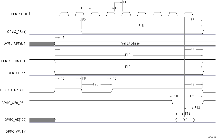
A. In GPMC_CSn[x], x is equal to 0, 1, 2 or
3.
B. In GPMC_WAIT[x], x is equal to 0 or
1.
Figure 6-48 GPMC and NOR
Flash—Synchronous Single Read—(GpmcFCLKDivider = 0) 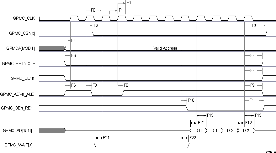
A. In GPMC_CSn[x], x is equal to 0, 1, 2 or
3.
B. In GPMC_WAIT[x], x is equal to 0 or
1.
Figure 6-49 GPMC and NOR
Flash—Synchronous Burst Read—4x16-bit (GpmcFCLKDivider = 0) 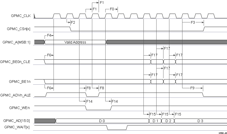
A. In GPMC_CSn[x], x is equal to 0, 1, 2 or
3.
B. In GPMC_WAIT[x], x is equal to 0 or
1.
Figure 6-50 GPMC and NOR
Flash—Synchronous Burst Write—(GpmcFCLKDivider > 0) 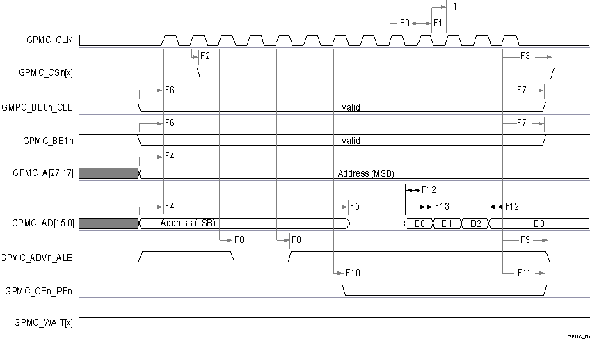
A. In GPMC_CSn[x], x is equal to 0, 1, 2 or
3.
B. In GPMC_WAIT[x], x is equal to 0 or
1.
Figure 6-51 GPMC and
Multiplexed NOR Flash—Synchronous Burst Read 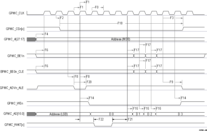
A. In GPMC_CSn[x], x is equal to 0, 1, 2 or
3.
B. In GPMC_WAIT[x], x is equal to 0 or
1.
Figure 6-52 GPMC and
Multiplexed NOR Flash—Synchronous Burst Write