ZHCSRW0A February 2023 – August 2023 AM68 , AM68A
PRODUCTION DATA
- 1
- 1 特性
- 2 应用
- 3 说明
- 4 Revision History
- 5 Device Comparison
-
6 Terminal Configuration and Functions
- 6.1 Pin Diagrams
- 6.2 Pin Attributes
- 6.3
Signal Descriptions
- 14
- 6.3.1 ADC
- 6.3.2 DDRSS
- 6.3.3 GPIO
- 6.3.4 I2C
- 6.3.5 I3C
- 6.3.6 MCAN
- 6.3.7 MCSPI
- 6.3.8 UART
- 6.3.9 MDIO
- 6.3.10 CPSW2G
- 6.3.11 ECAP
- 6.3.12 EQEP
- 6.3.13 EPWM
- 6.3.14 USB
- 6.3.15 Display Port
- 6.3.16 Hyperlink
- 6.3.17 PCIE
- 6.3.18 SERDES
- 6.3.19 DSI
- 6.3.20 CSI
- 6.3.21 MCASP
- 6.3.22 DMTIMER
- 6.3.23 CPTS
- 6.3.24 DSS
- 6.3.25 GPMC
- 6.3.26 MMC
- 6.3.27 OSPI
- 6.3.28 Hyperbus
- 6.3.29 Emulation and Debug
- 6.3.30 System and Miscellaneous
- 6.3.31 Power
- 6.4 Connection for Unused Pins
-
7 Specifications
- 7.1 绝对最大额定值
- 7.2 ESD Ratings
- 7.3 Recommended Operating Conditions
- 7.4 Power-On-Hour (POH) Limits
- 7.5 Operating Performance Points
- 7.6
Electrical Characteristics
- 7.6.1 I2C, Open-Drain, Fail-Safe (I2C OD FS) Electrical Characteristics
- 7.6.2 Fail-Safe Reset (FS Reset) Electrical Characteristics
- 7.6.3 HFOSC/LFOSC Electrical Characteristics
- 7.6.4 eMMCPHY Electrical Characteristics
- 7.6.5 SDIO Electrical Characteristics
- 7.6.6 CSI2/DSI D-PHY Electrical Characteristics
- 7.6.7 ADC12B Electrical Characteristics
- 7.6.8 LVCMOS Electrical Characteristics
- 7.6.9 USB2PHY Electrical Characteristics
- 7.6.10 SerDes 2-L-PHY/4-L-PHY Electrical Characteristics
- 7.6.11 UFS M-PHY Electrical Characteristics
- 7.6.12 eDP/DP AUX-PHY Electrical Characteristics
- 7.6.13 DDR0 Electrical Characteristics
- 7.7 VPP Specifications for One-Time Programmable (OTP) eFuses
- 7.8 Thermal Resistance Characteristics
- 7.9 Temperature Sensor Characteristics
- 7.10
Timing and Switching Characteristics
- 7.10.1 Timing Parameters and Information
- 7.10.2
Power Supply Sequencing
- 7.10.2.1 Power Supply Slew Rate Requirement
- 7.10.2.2 Combined MCU and Main Domains Power- Up Sequencing
- 7.10.2.3 Combined MCU and Main Domains Power- Down Sequencing
- 7.10.2.4 Isolated MCU and Main Domains Power- Up Sequencing
- 7.10.2.5 Isolated MCU and Main Domains Power- Down Sequencing
- 7.10.2.6 Independent MCU and Main Domains, Entry and Exit of MCU Only Sequencing
- 7.10.2.7 Independent MCU and Main Domains, Entry and Exit of DDR Retention State
- 7.10.2.8 Independent MCU and Main Domains, Entry and Exit of GPIO Retention Sequencing
- 7.10.3 System Timing
- 7.10.4
Clock Specifications
- 7.10.4.1 Input and Output Clocks / Oscillators
- 7.10.4.2 Output Clocks
- 7.10.4.3 PLLs
- 7.10.4.4 Module and Peripheral Clocks Frequencies
- 7.10.5
Peripherals
- 7.10.5.1 ATL
- 7.10.5.2
CPSW2G
- 7.10.5.2.1 CPSW2G MDIO Interface Timings
- 7.10.5.2.2 CPSW2G RMII Timings
- 7.10.5.2.3
CPSW2G RGMII Timings
- 7.10.5.2.3.1 RGMII[x]_RXC Timing Requirements – RGMII Mode
- 7.10.5.2.3.2 CPSW2G Timing Requirements for RGMII[x]_RD[3:0], and RGMII[x]_RCTL – RGMII Mode
- 7.10.5.2.3.3 CPSW2G RGMII[x]_TXC Switching Characteristics – RGMII Mode
- 7.10.5.2.3.4 RGMII[x]_TD[3:0], and RGMII[x]_TX_CTL Switching Characteristics – RGMII Mode
- 7.10.5.3 CSI-2
- 7.10.5.4 DDRSS
- 7.10.5.5 DSS
- 7.10.5.6 eCAP
- 7.10.5.7 EPWM
- 7.10.5.8 eQEP
- 7.10.5.9 GPIO
- 7.10.5.10 GPMC
- 7.10.5.11 HyperBus
- 7.10.5.12 I2C
- 7.10.5.13 I3C
- 7.10.5.14 MCAN
- 7.10.5.15 MCASP
- 7.10.5.16 MCSPI
- 7.10.5.17 MMCSD
- 7.10.5.18 CPTS
- 7.10.5.19 OSPI
- 7.10.5.20 PCIE
- 7.10.5.21 Timers
- 7.10.5.22 UART
- 7.10.5.23 USB
- 7.10.6 Emulation and Debug
- 8 Detailed Description
-
9 Applications,
Implementation, and Layout
- 9.1 Device Connection and Layout Fundamentals
- 9.2 Peripheral- and Interface-Specific Design Information
- 10Device and Documentation Support
- 11Mechanical, Packaging, and Orderable Information
7.10.5.10.1.2 GPMC and NOR Flash Switching Characteristics – Synchronous Mode
| NO.(2) | PARAMETER | DESCRIPTION | MODE(19) | MIN | MAX | MIN | MAX | UNIT |
|---|---|---|---|---|---|---|---|---|
| 100 MHz(23) | 133 MHz(23) | |||||||
| F0 | tc(clk) | Period, output clock GPMC_CLK(18) | div_by_1_mode; ; GPMC_FCLK_MUX; TIMEPARAGRANULARITY_X1 | 10 | 7.52 | ns | ||
| F1 | tw(clkH) | Typical pulse duration, output clock GPMC_CLK high | div_by_1_mode ; GPMC_FCLK_MUX; TIMEPARAGRANULARITY_X1 | 0.475*P(15)- 0.3 | 0.475*P(15)- 0.3 | ns | ||
| F1 | tw(clkL) | Typical pulse duration, output clock GPMC_CLK low | div_by_1_mode ; GPMC_FCLK_MUX; TIMEPARAGRANULARITY_X1 | 0.475*P(15)- 0.3 | 0.475*P(15)- 0.3 | ns | ||
| F2 | td(clkH-csnV) | Delay time, output clock GPMC_CLK rising edge to output chip select GPMC_CSn[i] transition(14) | div_by_1_mode ; GPMC_FCLK_MUX; TIMEPARAGRANULARITY_X1 no extra_delay | F(6)- 2.2 | F+3.75 | F(6)- 2.2 | F(6)+ 3.75 | ns |
| F3 | td(clkH-CSn[i]V) | Delay time, output clock GPMC_CLK rising edge to output chip select GPMC_CSn[i] invalid(14) | div_by_1_mode ; GPMC_FCLK_MUX; TIMEPARAGRANULARITY_X1 no extra_delay | E(5)- 2.2 | E(5)+ 3.75 | E(5)- 2.2 | E(5)+ 3.75 | ns |
| F4 | td(aV-clk) | Delay time, output address GPMC_A[27:1] valid to output clock GPMC_CLK first edge | div_by_1_mode ; GPMC_FCLK_MUX; TIMEPARAGRANULARITY_X1 | B(2)-2.3 | B(2)+4.5 | B(2)-2.3 | B(2)+4.5 | ns |
| F5 | td(clkH-aIV) | Delay time, output clock GPMC_CLK rising edge to output address GPMC_A[27:1] invalid | div_by_1_mode; GPMC_FCLK_MUX; TIMEPARAGRANULARITY_X1 | –2.3 | 4.5 | –2.3 | 4.5 | ns |
| F6 | td(be[x]nV-clk) | Delay time, output lower byte enable and command latch enable GPMC_BE0n_CLE, output upper byte enable GPMC_BE1n valid to output clock GPMC_CLK first edge | div_by_1_mode ; GPMC_FCLK_MUX; TIMEPARAGRANULARITY_X1 | B(2)-2.3 | B(2)+1.9 | B(2)-2.3 | B(2)+1.9 | ns |
| F7 | td(clkH-be[x]nIV) | Delay time, output clock GPMC_CLK rising edge to output lower byte enable and command latch enable GPMC_BE0n_CLE, output upper byte enable GPMC_BE1n invalid(11) | div_by_1_mode ; GPMC_FCLK_MUX; TIMEPARAGRANULARITY_X1 | D(4)-2.3 | D(4)+1.9 | D(4)-2.3 | D(4)+1.9 | ns |
| F7 | td(clkL-be[x]nIV) | Delay time, GPMC_CLK falling edge to GPMC_BE0n_CLE, GPMC_BE1n invalid(12) | div_by_1_mode ; GPMC_FCLK_MUX; TIMEPARAGRANULARITY_X1 | D(4)-2.3 | D(4)+1.9 | D(4)-2.3 | D(4)+1.9 | ns |
| F7 | td(clkL-be[x]nIV). | Delay time, GPMC_CLK falling edge to GPMC_BE0n_CLE, GPMC_BE1n invalid(13) | div_by_1_mode ; GPMC_FCLK_MUX; TIMEPARAGRANULARITY_X1 | D(4)-2.3 | D(4)+1.9 | D(4)-2.3 | D(4)+1.9 | ns |
| F8 | td(clkH-advn) | Delay time, output clock GPMC_CLK rising edge to output address valid and address latch enable GPMC_ADVn_ALE transition | div_by_1_mode ; GPMC_FCLK_MUX; TIMEPARAGRANULARITY_X1 no extra_delay | G(7)-2.3 | G(7)+4.5 | G(7)-2.3 | G(7)+4.5 | ns |
| F9 | td(clkH-advnIV) | Delay time, output clock GPMC_CLK rising edge to output address valid and address latch enable GPMC_ADVn_ALE invalid | div_by_1_mode; GPMC_FCLK_MUX; TIMEPARAGRANULARITY_X1 no extra_delay | D(4)-2.3 | D(4)+4.5 | D(4)-2.3 | D(4)+4.5 | ns |
| F10 | td(clkH-oen) | Delay time, output clock GPMC_CLK rising edge to output enable GPMC_OEn_REn transition | div_by_1_mode ; GPMC_FCLK_MUX; TIMEPARAGRANULARITY_X1 no extra_delay | H(8)-2.3 | H(8)+3.5 | H(8)-2.3 | H(8)+3.5 | ns |
| F11 | td(clkH-oenIV) | Delay time, output clock GPMC_CLK rising edge to output enable GPMC_OEn_REn invalid | div_by_1_mode ; GPMC_FCLK_MUX; TIMEPARAGRANULARITY_X1 no extra_delay | E(8)-2.3 | E(8)+3.5 | E(8)-2.3 | E(8)+ 3.5 | ns |
| F14 | td(clkH-wen) | Delay time, output clock GPMC_CLK rising edge to output write enable GPMC_WEn transition | div_by_1_mode ; GPMC_FCLK_MUX; TIMEPARAGRANULARITY_X1 no extra_delay | I(9)- 2.3 | I(9)+4.5 | I(9)- 2.3 | I(9)+4.5 | ns |
| F15 | td(clkH-do) | Delay time, output clock GPMC_CLK rising edge to output data GPMC_AD[15:0] transition(11) | div_by_1_mode ; GPMC_FCLK_MUX; TIMEPARAGRANULARITY_X1 | J(10)-2.3 | J(10)+2.7 | J(10)-2.3 | J(10)+2.7 | ns |
| F15 | td(clkL-do) | Delay time, GPMC_CLK falling edge to GPMC_AD[15:0] data bus transition(12) | div_by_1_mode ; GPMC_FCLK_MUX; TIMEPARAGRANULARITY_X1 | J(10)-2.3 | J(10)+2.7 | J(10)-2.3 | J(10)+2.7 | ns |
| F15 | td(clkL-do). | Delay time, GPMC_CLK falling edge to GPMC_AD[15:0] data bus transition(13) | div_by_1_mode ; GPMC_FCLK_MUX; TIMEPARAGRANULARITY_X1 | J(10)-2.3 | J(10)+2.7 | J(10)-2.3 | J(10)+2.7 | ns |
| F17 | td(clkH-be[x]n) | Delay time, output clock GPMC_CLK rising edge to output lower byte enable and command latch enable GPMC_BE0n_CLE transition(11) | div_by_1_mode ; GPMC_FCLK_MUX; TIMEPARAGRANULARITY_X1 | J(10)-2.3 | J(10)+1.9 | J(10)-2.3 | J(10)+1.9 | ns |
| F17 | td(clkL-be[x]n) | Delay time, GPMC_CLK falling edge to GPMC_BE0n_CLE, GPMC_BE1n transition(12) | div_by_1_mode ; GPMC_FCLK_MUX; TIMEPARAGRANULARITY_X1 | J(10)-2.3 | J(10)+1.9 | J(10)-2.3 | J(10)+1.9 | ns |
| F17 | td(clkL-be[x]n). | Delay time, GPMC_CLK falling edge to GPMC_BE0n_CLE, GPMC_BE1n transition(13) | div_by_1_mode ; GPMC_FCLK_MUX; TIMEPARAGRANULARITY_X1 | J(10)-2.3 | J(10)+1.9 | J(10)-2.3 | J(10)+1.9 | ns |
| F18 | tw(csnV) | Pulse duration, output chip select GPMC_CSn[i] low(14) | Read | A(1) | A(1) | ns | ||
| Write | A(1) | A(1) | ns | |||||
| F19 | tw(be[x]nV) | Pulse duration, output lower byte enable and command latch enable GPMC_BE0n_CLE, output upper byte enable GPMC_BE1n low | Read | C(3) | C(3) | ns | ||
| Write | C(3) | C(3) | ns | |||||
| F20 | tw(advnV) | Pulse duration, output address valid and address latch enable GPMC_ADVn_ALE low | Read | K(16) | K(16) | ns | ||
| Write | K(16) | K(16) | ns | |||||
(1) For single read: A = (CSRdOffTime - CSOnTime) × (TimeParaGranularity + 1) × GPMC_FCLK(17)
For burst read: A = (CSRdOffTime - CSOnTime + (n - 1) × PageBurstAccessTime) × (TimeParaGranularity + 1) × GPMC_FCLK(17)
For burst write: A = (CSWrOffTime - CSOnTime + (n - 1) × PageBurstAccessTime) × (TimeParaGranularity + 1) × GPMC_FCLK(17)
With n being the page burst access number.
For burst read: A = (CSRdOffTime - CSOnTime + (n - 1) × PageBurstAccessTime) × (TimeParaGranularity + 1) × GPMC_FCLK(17)
For burst write: A = (CSWrOffTime - CSOnTime + (n - 1) × PageBurstAccessTime) × (TimeParaGranularity + 1) × GPMC_FCLK(17)
With n being the page burst access number.
(2) B = ClkActivationTime × GPMC_FCLK(17)
(3) For single read: C = RdCycleTime × (TimeParaGranularity + 1) × GPMC_FCLK(17)
For burst read: C = (RdCycleTime + (n - 1) × PageBurstAccessTime) × (TimeParaGranularity + 1) × GPMC_FCLK(17)
For burst write: C = (WrCycleTime + (n - 1) × PageBurstAccessTime) × (TimeParaGranularity + 1) × GPMC_FCLK(17)
With n being the page burst access number.
For burst read: C = (RdCycleTime + (n - 1) × PageBurstAccessTime) × (TimeParaGranularity + 1) × GPMC_FCLK(17)
For burst write: C = (WrCycleTime + (n - 1) × PageBurstAccessTime) × (TimeParaGranularity + 1) × GPMC_FCLK(17)
With n being the page burst access number.
(4) For single read: D = (RdCycleTime - AccessTime) × (TimeParaGranularity + 1) × GPMC_FCLK(17)
For burst read: D = (RdCycleTime - AccessTime) × (TimeParaGranularity + 1) × GPMC_FCLK(17)
For burst write: D = (WrCycleTime - AccessTime) × (TimeParaGranularity + 1) × GPMC_FCLK(17)
For burst read: D = (RdCycleTime - AccessTime) × (TimeParaGranularity + 1) × GPMC_FCLK(17)
For burst write: D = (WrCycleTime - AccessTime) × (TimeParaGranularity + 1) × GPMC_FCLK(17)
(5) For single read: E = (CSRdOffTime - AccessTime) × (TimeParaGranularity + 1) × GPMC_FCLK(17)
For burst read: E = (CSRdOffTime - AccessTime) × (TimeParaGranularity + 1) × GPMC_FCLK(17)
For burst write: E = (CSWrOffTime - AccessTime) × (TimeParaGranularity + 1) × GPMC_FCLK(17)
For burst read: E = (CSRdOffTime - AccessTime) × (TimeParaGranularity + 1) × GPMC_FCLK(17)
For burst write: E = (CSWrOffTime - AccessTime) × (TimeParaGranularity + 1) × GPMC_FCLK(17)
(6) For csn falling edge (CS activated):
- Case GPMCFCLKDIVIDER = 0:
- F = 0.5 × CSExtraDelay × GPMC_FCLK(17)
- Case GPMCFCLKDIVIDER = 1:
- Case GPMCFCLKDIVIDER = 2:
(7) For ADV falling edge (ADV activated):
For ADV rising edge (ADV deactivated) in Reading mode:
For ADV rising edge (ADV deactivated) in Writing mode:
- Case GPMCFCLKDIVIDER = 0:
- G = 0.5 × ADVExtraDelay × GPMC_FCLK(17)
- Case GPMCFCLKDIVIDER = 1:
- Case GPMCFCLKDIVIDER = 2:
- G = 0.5 × ADVExtraDelay × GPMC_FCLK(17) if ((ADVOnTime - ClkActivationTime) is a multiple of 3)
- G = (1 + 0.5 × ADVExtraDelay) × GPMC_FCLK(17) if ((ADVOnTime - ClkActivationTime - 1) is a multiple of 3)
- G = (2 + 0.5 × ADVExtraDelay) × GPMC_FCLK(17) if ((ADVOnTime - ClkActivationTime - 2) is a multiple of 3)
For ADV rising edge (ADV deactivated) in Reading mode:
- Case GPMCFCLKDIVIDER = 0:
- G = 0.5 × ADVExtraDelay × GPMC_FCLK(17)
- Case GPMCFCLKDIVIDER = 1:
- Case GPMCFCLKDIVIDER = 2:
- G = 0.5 × ADVExtraDelay × GPMC_FCLK(17) if ((ADVRdOffTime - ClkActivationTime) is a multiple of 3)
- G = (1 + 0.5 × ADVExtraDelay) × GPMC_FCLK(17) if ((ADVRdOffTime - ClkActivationTime - 1) is a multiple of 3)
- G = (2 + 0.5 × ADVExtraDelay) × GPMC_FCLK(17) if ((ADVRdOffTime - ClkActivationTime - 2) is a multiple of 3)
For ADV rising edge (ADV deactivated) in Writing mode:
- Case GPMCFCLKDIVIDER = 0:
- G = 0.5 × ADVExtraDelay × GPMC_FCLK(17)
- Case GPMCFCLKDIVIDER = 1:
- Case GPMCFCLKDIVIDER = 2:
- G = 0.5 × ADVExtraDelay × GPMC_FCLK(17) if ((ADVWrOffTime - ClkActivationTime) is a multiple of 3)
- G = (1 + 0.5 × ADVExtraDelay) × GPMC_FCLK(17) if ((ADVWrOffTime - ClkActivationTime - 1) is a multiple of 3)
- G = (2 + 0.5 × ADVExtraDelay) × GPMC_FCLK(17) if ((ADVWrOffTime - ClkActivationTime - 2) is a multiple of 3)
(8) For OE falling edge (OE activated) and IO DIR rising edge (Data Bus input direction):
For OE rising edge (OE deactivated):
- Case GPMCFCLKDIVIDER = 0:
- H = 0.5 × OEExtraDelay × GPMC_FCLK(17)
- Case GPMCFCLKDIVIDER = 1:
- Case GPMCFCLKDIVIDER = 2:
For OE rising edge (OE deactivated):
- Case GPMCFCLKDIVIDER = 0:
- H = 0.5 × OEExtraDelay × GPMC_FCLK(17)
- Case GPMCFCLKDIVIDER = 1:
- Case GPMCFCLKDIVIDER = 2:
- H = 0.5 × OEExtraDelay × GPMC_FCLK(17) if ((OEOffTime - ClkActivationTime) is a multiple of 3)
- H = (1 + 0.5 × OEExtraDelay) × GPMC_FCLK(17) if ((OEOffTime - ClkActivationTime - 1) is a multiple of 3)
- H = (2 + 0.5 × OEExtraDelay) × GPMC_FCLK(17) if ((OEOffTime - ClkActivationTime - 2) is a multiple of 3)
(9) For WE falling edge (WE activated):
For WE rising edge (WE deactivated):
- Case GPMCFCLKDIVIDER = 0:
- I = 0.5 × WEExtraDelay × GPMC_FCLK(17)
- Case GPMCFCLKDIVIDER = 1:
- Case GPMCFCLKDIVIDER = 2:
For WE rising edge (WE deactivated):
- Case GPMCFCLKDIVIDER = 0:
- I = 0.5 × WEExtraDelay × GPMC_FCLK (17)
- Case GPMCFCLKDIVIDER = 1:
- Case GPMCFCLKDIVIDER = 2:
- I = 0.5 × WEExtraDelay × GPMC_FCLK(17) if ((WEOffTime - ClkActivationTime) is a multiple of 3)
- I = (1 + 0.5 × WEExtraDelay) × GPMC_FCLK(17) if ((WEOffTime - ClkActivationTime - 1) is a multiple of 3)
- I = (2 + 0.5 × WEExtraDelay) × GPMC_FCLK(17) if ((WEOffTime - ClkActivationTime - 2) is a multiple of 3)
(10) J = GPMC_FCLK(17)
(11) First transfer only for CLK DIV 1 mode.
(12) Half cycle; for all data after initial transfer for CLK DIV 1 mode.
(13) Half cycle of GPMC_CLKOUT; for all data for modes other than CLK DIV 1 mode. GPMC_CLKOUT divide down from GPMC_FCLK.
(14) In GPMC_CSn[i], i
is equal to 0, 1, 2, or 3. In GPMC_WAIT[j], j is equal to 0, 1, 2, or 3.
(15) P = GPMC_CLK period in ns
(16) For read: K = (ADVRdOffTime - ADVOnTime) × (TimeParaGranularity + 1) × GPMC_FCLK(17)
For write: K = (ADVWrOffTime - ADVOnTime) × (TimeParaGranularity + 1) × GPMC_FCLK(17)
For write: K = (ADVWrOffTime - ADVOnTime) × (TimeParaGranularity + 1) × GPMC_FCLK(17)
(17) GPMC_FCLK is general-purpose memory controller internal functional clock period in ns.
(18) Related to the GPMC_CLK output clock maximum and minimum frequencies programmable in the GPMC module by setting the GPMC_CONFIG1_i configuration register bit field GPMCFCLKDIVIDER.
(19) For div_by_1_mode:
For no extra_delay:
- GPMC_CONFIG1_i register:
GPMCFCLKDIVIDER = 0h:
- GPMC_CLK frequency = GPMC_FCLK frequency
- CTRLMMR_GPMC_CLKSEL[1-0] CLK_SEL = 01 = PER1_PLL_CLKOUT / 3 = 300 / 3 = 100 MHz
- GPMC_CONFIG1_i Register: TIMEPARAGRANULARITY = 0h = x1 latencies (affecting RD/WRCYCLETIME, RD/WRACCESSTIME, PAGEBURSTACCESSTIME, CSONTIME, CSRD/WROFFTIME, ADVONTIME, ADVRD/WROFFTIME, OEONTIME, OEOFFTIME, WEONTIME, WEOFFTIME, CYCLE2CYCLEDELAY, BUSTURNAROUND, TIMEOUTSTARTVALUE, WRDATAONADMUXBUS)
For no extra_delay:
- GPMC_CONFIG2_i Register: CSEXTRADELAY = 0h = CSn Timing control signal is not delayed
- GPMC_CONFIG4_i Register: WEEXTRADELAY = 0h = nWE timing control signal is not delayed
- GPMC_CONFIG4_i Register: OEEXTRADELAY = 0h = nOE timing control signal is not delayed
- GPMC_CONFIG3_i Register: ADVEXTRADELAY = 0h = nADV timing control signal is not delayed
(23) For 100 MHz:
- CTRLMMR_GPMC_CLKSEL[1-0] CLK_SEL = 01 = MAIN_PLL2_HSDIV1_CLKOUT / 3
- CTRLMMR_GPMC_CLKSEL[1-0] CLK_SEL = 00 = MAIN_PLL0_HSDIV3_CLKOUT
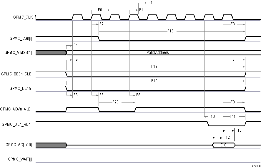
A. In GPMC_CSn[i], i is equal to 0, 1, 2 or
3.
B. In GPMC_WAIT[j], j is equal to 0, 1, 2,
or 3.
Figure 7-51 GPMC and NOR
Flash — Synchronous Single Read (GPMCFCLKDIVIDER = 0) 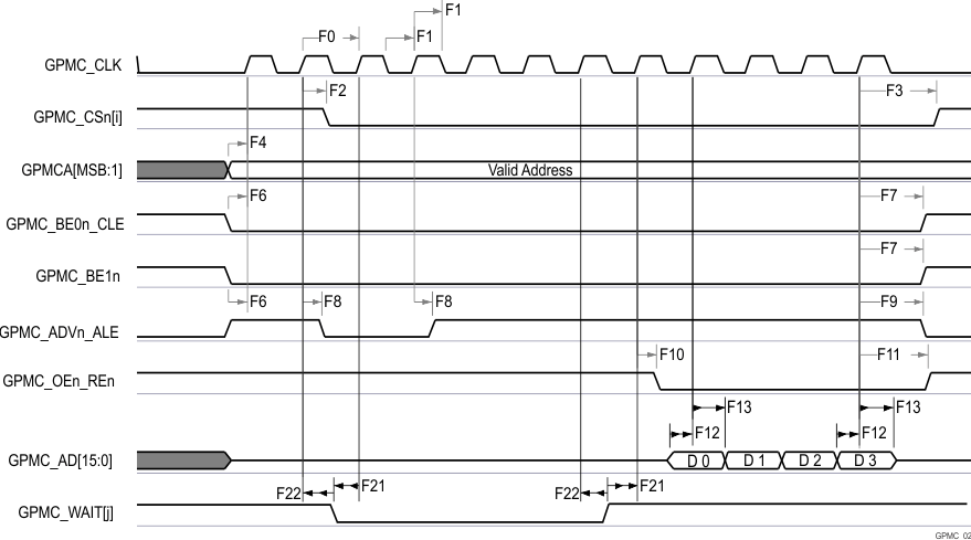
A. In GPMC_CSn[i], i is equal to 0, 1, 2 or
3.
B. In GPMC_WAIT[j], j is equal to 0, 1, 2,
or 3.
Figure 7-52 GPMC and NOR
Flash — Synchronous Burst Read — 4x16–bit (GPMCFCLKDIVIDER = 0) 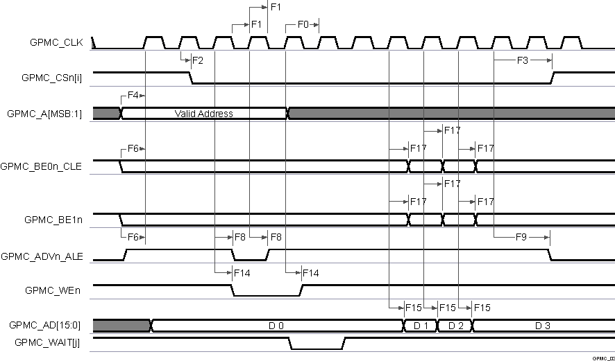
A. In GPMC_CSn[i], i is equal to 0, 1, 2 or
3.
B. In GPMC_WAIT[j], j is equal to 0, 1, 2,
or 3.
Figure 7-53 GPMC and NOR
Flash—Synchronous Burst Write (GPMCFCLKDIVIDER = 0) 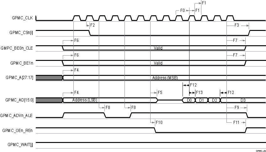
A. In GPMC_CSn[i], i is equal to 0, 1, 2 or
3.
B. In GPMC_WAIT[j], j is equal to 0, 1, 2,
or 3.
Figure 7-54 GPMC and
Multiplexed NOR Flash — Synchronous Burst Read 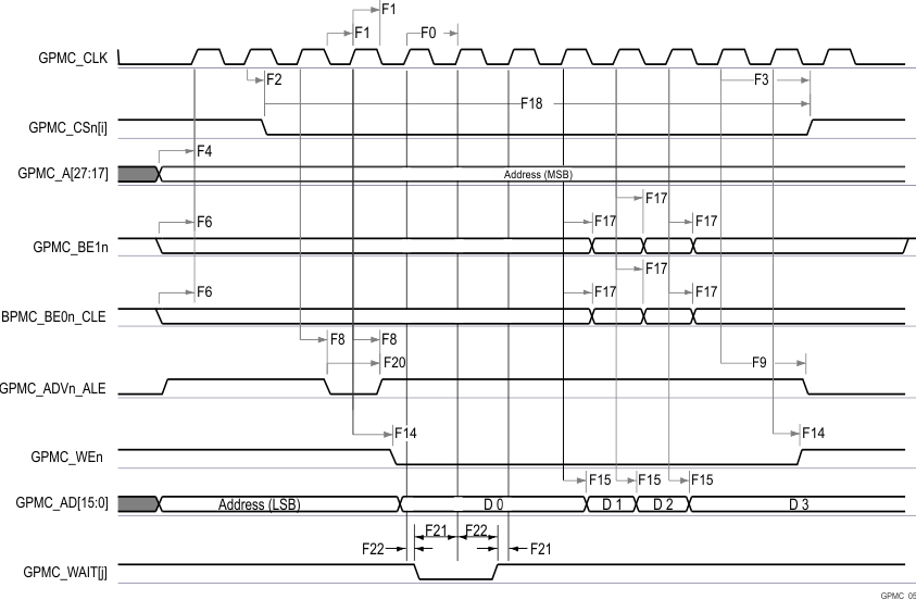
A. In GPMC_CSn[i], i is equal to 0, 1, 2 or
3.
B. In GPMC_WAIT[j], j is equal to 0, 1, 2,
or 3.
Figure 7-55 GPMC and
Multiplexed NOR Flash — Synchronous Burst Write