SBASB14 October 2024 AMC0311S-Q1
ADVANCE INFORMATION
- 1
- 1 Features
- 2 Applications
- 3 Description
- 4 Device Comparison Table
- 5 Pin Configuration and Functions
-
6 Specifications
- 6.1 Absolute Maximum Ratings
- 6.2 ESD Ratings
- 6.3 Recommended Operating Conditions
- 6.4 Thermal Information (D Package)
- 6.5 Thermal Information (DWV Package)
- 6.6 Power Ratings
- 6.7 Insulation Specifications (Basic Isolation)
- 6.8 Insulation Specifications (Reinforced Isolation)
- 6.9 Safety-Related Certifications (Basic Isolation)
- 6.10 Safety-Related Certifications (Reinforced Isolation)
- 6.11 Safety Limiting Values (D Package)
- 6.12 Safety Limiting Values (DWV Package)
- 6.13 Electrical Characteristics
- 6.14 Switching Characteristics
- 6.15 Timing Diagram
- 7 Detailed Description
- 8 Application and Implementation
- 9 Power Supply Recommendations
- 10Layout
- 11Device and Documentation Support
- 12Revision History
- 13Mechanical, Packaging, and Orderable Information
7.3.3 Analog Output
The AMC0x11S-Q1 provides a single-ended analog output voltage that is proportional to the input voltage. The output is referred to GND2 and is galvanically isolated from the input of the device. The output is designed to connect directly to the input of an ADC.
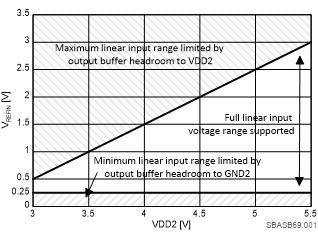
The output buffer requires a minimum headroom of 250mV for linear operation. Therefore, with REFIN shorted to GND2, the device shows non-linear behavior for input voltages near 0V. To extend the linear input range to 0V, connect a reference voltage to the REFIN pin that is ≥250mV. The voltage applied to the REFIN pin is added to the output voltage as an offset and provides headroom for the output buffer. Connect the REFIN pin to GND2 if no offset is required. The output voltage of the AMC0x11S-Q1 is equal to:
Figure 7-2 shows the recommended input range of the reference voltage for linear operation. Figure 7-3 shows the input-to-output transfer characteristic of the device.
 Figure 7-2 Recommended Reference Voltage Range for Linear
Operation
 Figure 7-3 Input
to Output Transfer Curve of the AMC0x11S-Q1 Left: REFIN shorted to GND2.
Right: VREFIN = 250mV