ZHCSIP8B August 2018 – April 2020 AMC1035
PRODUCTION DATA.
6.6 Switching Characteristics
over operating free-air temperature range (unless otherwise noted)| PARAMETER | TEST CONDITIONS | MIN | TYP | MAX | UNIT | |
|---|---|---|---|---|---|---|
| fCLKIN | CLKIN clock frequency | MCE = 0 | 9 | 20 | 21 | MHz |
| MCE = 1 | 9 | 10 | 11 | |||
| DutyCycle | CLKIN clock duty cycle(1) | 40% | 50% | 60% | ||
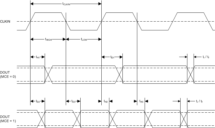
| tH1 | DOUT hold time after rising edge of CLKIN | MCE = 0, CLOAD = 15 pF | 6 | ns | ||
| tH2 | DOUT hold time after rising edge of CLKIN | MCE = 1, CLOAD = 15 pF | 6 | 23 | ns | |
| tH3 | DOUT hold time after falling edge of CLKIN | MCE = 1, CLOAD = 15 pF | 10 | 26 | ns | |
| tD1 | Rising edge of CLKIN to DOUT valid delay | MCE = 0, CLOAD = 15 pF | 25 | ns | ||
| tD2 | Rising edge of CLKIN to DOUT valid delay | MCE = 1, CLOAD = 15 pF | 11 | 27 | ns | |
| tD3 | Falling edge of CLKIN to DOUT valid delay | MCE = 1, CLOAD = 15 pF | 15 | 30 | ns | |
| tr | DOUT rise time | 10% to 90%, 3.0 V ≤ VDD ≤ 3.6 V, CLOAD = 15 pF | 2.5 | 5 | ns | |
| 10% to 90%, 4.5 V ≤ VDD ≤ 5.5 V, CLOAD = 15 pF | 1.5 | 3.5 | ||||
| tf | DOUT fall time | 90% to 10%, 3.0 V ≤ VDD ≤ 3.6 V, CLOAD = 15 pF | 2.5 | 5.8 | ns | |
| 90% to 10%, 4.5 V ≤ VDD ≤ 5.5 V, CLOAD = 15 pF | 1.8 | 4.4 | ||||
| tASTART | Analog startup time | VDD step to 3.0 V, 0.1% settling, CLKIN applied | 0.25 | ms | ||
(1) The duty cycle of DOUT equals the clock duty cycle of the applied CLKIN signal.
 Figure 1. Digital Interface Timing
  Figure 2. Device Startup Timing