ZHCS161D April 2011 – July 2015 AMC1200
PRODUCTION DATA.
- 1 特性
- 2 应用
- 3 说明
- 4 修订历史记录
- 5 Pin Configuration and Functions
- 6 Specifications
- 7 Detailed Description
- 8 Application and Implementation
- 9 Power Supply Recommendations
- 10Layout
- 11器件和文档支持
- 12机械、封装和可订购信息
封装选项
机械数据 (封装 | 引脚)
散热焊盘机械数据 (封装 | 引脚)
- DUB|8
订购信息
8 Application and Implementation
NOTE
Information in the following applications sections is not part of the TI component specification, and TI does not warrant its accuracy or completeness. TI’s customers are responsible for determining suitability of components for their purposes. Customers should validate and test their design implementation to confirm system functionality.
8.1 Application Information
The AMC1200 and AMC1200B devices offer unique linearity, high input common mode rejection, low DC errors and low temperature drift. These features make the AMC1200 a robust, high-performance isolation amplifier for industrial applications where high voltage isolation is required.
8.2 Typical Applications
8.2.1 Motor Control
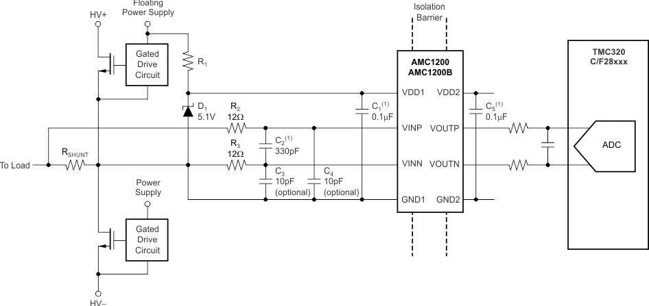
Figure 32 shows a typical operation of the AMC1200 and AMC1200B devices in a motor-control application. Measurement of the motor phase current is done through the shunt resistor, RSHUNT (in this case, a two-terminal shunt).

The high-side power supply (VDD1) for the AMC1200 and AMC1200B are derived from the power supply of the upper gate driver. Further details are provided in the Power Supply Recommendations section.
The high transient immunity of the AMC1200 and AMC1200B ensures reliable and accurate operation even in high-noise environments such as the power stages of the motor drives.
As shown in Figure 37, TI recommends placing the bypass and filter capacitors as close as possible to the AMC device to ensure best performance.
8.2.1.1 Design Requirements
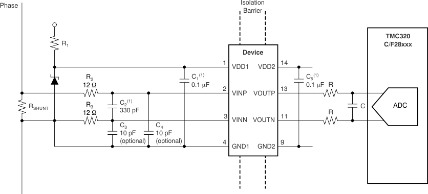
For better performance, the differential input signal is filtered using RC filters (components R2, R3, and C2). Optionally, C3 and C4 can be used to reduce charge dumping from the inputs. In this case, take care when choosing the quality of these capacitors; mismatch in values of these capacitors leads to a common mode error at the modulator input. If implemented, TI recommends using NP0 capacitors for C2, C3 and C4.
 Figure 33. Shunt-Based Current Sensing with the AMC1200
Similar to the current measurements, isolated voltage measurements can be performed as described in the .
8.2.1.2 Detailed Design Procedure
The floating ground reference (GND1) is derived from the end of the shunt resistor, which is connected to the negative input of the AMC1200 (VINN). If a four-terminal shunt is used, the inputs of the AMC1200 are connected to the inner leads and GND1 is connected to one of the outer shunt leads. The differential input of the AMC1200 ensures accurate operation even in noisy environments.
TI recommends limiting the value of resistors R2 and R3 to less than 24 Ω to avoid the incomplete settling of the AMC1200 input circuitry. The section provides more details on the AMC1200 input circuitry.
The differential output of the AMC1200 can either directly drive an analog-to-digital converter (ADC) input or can be further filtered before being processed by the ADC. For more information on the general procedure to design the filtering and driving stages for SAR ADCs, consult the TI Precision Designs 18 bit, 1Msps Data Acquisition Block Optimized for Lowest Distortion and Noise (SLAU515), and 18 bit Data Acquisition Block Optimized for Lowest Power (SLAU513) available for download at www.ti.com
8.2.1.3 Application Curve
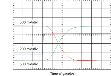
In frequency inverter applications the power switches must be protected in case of an overcurrent condition. To allow fast powering off of the system, low delay caused by the isolation amplifier is required. Figure 34 shows the typical full-scale step response of the AMC1200.

8.2.2 Isolated Voltage Measurement
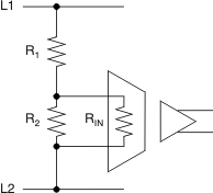
The AMC1200 and AMC1200B can also be used for isolated voltage measurement applications, as shown in a simplified way in Figure 35. In such applications, usually a resistor divider (R1 and R2 in Figure 35) is used to match the relatively small input voltage range of the AMC device. R2 and the input resistance RIN of the AMC1200 also create a resistance divider that results in additional gain error. With the assumption that R1 and RIN have a considerably higher value than R2, the resulting total gain error can be estimated using Equation 1:

where
- GERR = the gain error of AMC device.
 Figure 35. Voltage Measurement Application