ZHCS142F April 2011 – February 2020 AMC1204
PRODUCTION DATA.
- 1 特性
- 2 应用
- 3 说明
- 4 修订历史记录
- 5 Pin Configuration and Functions
-
6 Specifications
- 6.1 Absolute Maximum Ratings
- 6.2 ESD Ratings
- 6.3 Recommended Operating Conditions
- 6.4 Thermal Information
- 6.5 Power Ratings
- 6.6 Insulation Specifications
- 6.7 Safety-Related Certifications
- 6.8 Safety Limiting Values
- 6.9 Electrical Characteristics
- 6.10 Timing Requirements
- 6.11 Insulation Characteristics Curves
- 6.12 Typical Characteristics
- 7 Detailed Description
- 8 Application and Implementation
- 9 Power Supply Recommendations
- 10Layout
- 11器件和文档支持
- 12机械、封装和可订购信息
封装选项
机械数据 (封装 | 引脚)
散热焊盘机械数据 (封装 | 引脚)
- DW|16
订购信息
7.3.2 Modulator
The modulator topology of the AMC1204 and AMC1204B is fundamentally a second-order, switched-capacitor, ΔΣ modulator, such as the one conceptualized in Figure 45. The analog input voltage (X(t)) and the output of the 1-bit digital-to-analog converter (DAC) are differentiated, providing an analog voltage (X2) at the input of the first integrator or modulator stage. The output of the first integrator is further differentiated with the DAC output; the resulting voltage (X3) feeds the input of the second integrator stage. When the value of the integrated signal (X4) at the output of the second stage equals the comparator reference voltage, the output of the comparator switches from high to low, or vice versa, depending on its previous state. In this case, the 1-bit DAC responds on the next clock pulse by changing its analog output voltage (X6), causing the integrators to progress in the opposite direction, while forcing the value of the integrator output to track the average of the input.
 Figure 45. Block Diagram Of A Second-Order Modulator
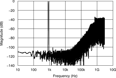
 The modulator shifts the quantization noise to high frequencies, as shown in Figure 46; therefore, a low-pass digital filter should be used at the output of the device to increase the overall performance. This filter is also used to convert from the 1-bit data stream at a high sampling rate into a higher-bit data word at a lower rate (decimation). A digital signal processor (DSP), microcontroller (µC), or field programmable gate array (FPGA) can be used to implement the filter.
TI's microcontroller family TMS320F28x7x offers a suitable programmable, hardwired filter structure termed a sigma-delta filter module (SDFM) optimized for usage with the AMC1204, AMC1304 and AMC1305 devices. Also, the SD24_B converters on the MSP430F677x microcontrollers offer a path to directly access the integrated sinc-filters, thus offering a system-level solution for multichannel isolated current sensing. Another option is to use a suitable application-specific device such as the AMC1210, a four-channel digital sinc-filter.
 Figure 46. Quantization Noise Shaping