ZHCSFZ4 February 2017 AMC1304L05-Q1 , AMC1304L25-Q1 , AMC1304M05-Q1 , AMC1304M25-Q1
PRODUCTION DATA.
- 1 特性
- 2 应用
- 3 说明
- 4 修订历史记录
- 5 Device Comparison Table
- 6 Pin Configurations and Functions
-
7 Specifications
- 7.1 Absolute Maximum Ratings
- 7.2 ESD Ratings
- 7.3 Recommended Operating Conditions
- 7.4 Thermal Information
- 7.5 Power Ratings
- 7.6 Insulation Specifications
- 7.7 Safety-Related Certifications
- 7.8 Safety Limiting Values
- 7.9 Electrical Characteristics: AMC1304x05-Q1
- 7.10 Electrical Characteristics: AMC1304x25-Q1
- 7.11 Switching Characteristics
- 7.12 Insulation Characteristics Curves
- 7.13 Typical Characteristics
- 8 Detailed Description
- 9 Application and Implementation
- 10Power-Supply Recommendations
- 11Layout
- 12器件和文档支持
- 13机械、封装和可订购信息
7 Specifications
7.1 Absolute Maximum Ratings
over the operating ambient temperature range (unless otherwise noted)(1)| MIN | MAX | UNIT | ||
|---|---|---|---|---|
| Supply voltage | DVDD to DGND | –0.3 | 6.5 | V |
| LDO input voltage | LDOIN to AGND | –0.3 | 26 | V |
| Analog input voltage at AINP, AINN | AGND – 6 | 3.7 | V | |
| Digital input voltage at CLKIN, CLKIN_N | DGND – 0.3 | DVDD + 0.3 | V | |
| Input current to any pin except supply pins | –10 | 10 | mA | |
| Junction temperature, TJ | 150 | °C | ||
| Storage temperature, Tstg | –65 | 150 | °C | |
(1) Stresses beyond those listed under Absolute Maximum Ratings may cause permanent damage to the device. These are stress ratings only, and do not imply functional operation of the device at these or any other conditions beyond those indicated. Exposure to absolute-maximum-rated conditions for extended periods may affect device reliability.
7.2 ESD Ratings
| VALUE | UNIT | |||
|---|---|---|---|---|
| V(ESD) | Electrostatic discharge | Human body model (HBM), per AEC Q100-002(1) | ±2500 | V |
| Charged device model (CDM), per AEC Q100-011 | ±1000 | |||
(1) AEC Q100-002 indicates HBM stressing is done in accordance with the ANSI/ESDA/JEDEC JS-001 specification.
7.3 Recommended Operating Conditions
over operating free-air temperature range (unless otherwise noted)| MIN | NOM | MAX | UNIT | ||
|---|---|---|---|---|---|
| LDOIN | LDO input supply voltage (LDOIN pin) | 4.0 | 15.0 | 18.0 | V |
| DVDD | Digital (controller-side) supply voltage (DVDD pin) | 3.0 | 3.3 | 5.5 | V |
| TA | Operating ambient temperature range | –40 | 125 | °C | |
7.4 Thermal Information
| THERMAL METRIC (1) | AMC1304x-Q1 | UNIT | |
|---|---|---|---|
| DW (SOIC) | |||
| 16 PINS | |||
| RθJA | Junction-to-ambient thermal resistance | 80.2 | °C/W |
| RθJC(top) | Junction-to-case (top) thermal resistance | 40.5 | °C/W |
| RθJB | Junction-to-board thermal resistance | 45.1 | °C/W |
| ψJT | Junction-to-top characterization parameter | 11.9 | °C/W |
| ψJB | Junction-to-board characterization parameter | 44.5 | °C/W |
| RθJC(bot) | Junction-to-case (bottom) thermal resistance | n/a | °C/W |
(1) For more information about traditional and new thermal metrics, see the Semiconductor and IC Package Thermal Metrics application report.
7.5 Power Ratings
| PARAMETER | TEST CONDITIONS | VALUE | UNIT | |
|---|---|---|---|---|
| PD | Maximum power dissipation (both sides) | LDOIN = 18 V, DVDD = 5.5 V | 161 | mW |
| PD1 | Maximum power dissipation (high-side supply) | LDOIN = 18 V | 117 | mW |
| PD2 | Maximum power dissipation (low-side supply) | DVDD = 5.5 V, LVDS, RLOAD = 100 Ω | 44 | mW |
7.6 Insulation Specifications
| PARAMETER | TEST CONDITIONS | VALUE | UNIT | |
|---|---|---|---|---|
| GENERAL | ||||
| CLR | Minimum air gap (clearance)(1) | Shortest pin-to-pin distance through air | ≥ 8 | mm |
| CPG | Minimum external tracking (creepage)(1) | Shortest pin-to-pin distance across the package surface | ≥ 8 | mm |
| DTI | Distance through insulation | Minimum internal gap (internal clearance) of the double insulation (2 × 0.0135 mm) | 0.027 | mm |
| CTI | Comparative tracking index | DIN EN 60112 (VDE 0303-11); IEC 60112 | ≥ 600 | V |
| Material group | According to IEC 60664-1 | I | ||
| Overvoltage category per IEC 60664-1 | Rated mains voltage ≤ 300 VRMS | I-IV | ||
| Rated mains voltage ≤ 600 VRMS | I-III | |||
| Rated mains voltage ≤ 1000 VRMS | I-II | |||
| DIN V VDE V 0884-10 (VDE V 0884-10): 2006-12(2) | ||||
| VIORM | Maximum repetitive peak isolation voltage | At ac voltage (bipolar or unipolar) | 1414 | VPK |
| VIOWM | Maximum-rated isolation working voltage | At ac voltage (sine wave) | 1000 | VRMS |
| At dc voltage | 1500 | VDC | ||
| VIOTM | Maximum transient isolation voltage | VTEST = VIOTM, t = 60 s (qualification test) | 7000 | VPK |
| VTEST = 1.2 x VIOTM, t = 1 s (100% production test) | 8400 | |||
| VIOSM | Maximum surge isolation voltage(3) | Test method per IEC 60065, 1.2/50-μs waveform, VTEST = 1.6 x VIOSM = 10000 VPK (qualification) | 6250 | VPK |
| qpd | Apparent charge(4) | Method a, after input/output safety test subgroup 2 / 3, Vini = VIOTM, tini = 60 s, Vpd(m) = 1.2 x VIORM = 1697 VPK, tm = 10 s | ≤ 5 | pC |
| Method a, after environmental tests subgroup 1, Vini = VIOTM, tini = 60 s, Vpd(m) = 1.6 x VIORM = 2263 VPK, tm = 10 s | ≤ 5 | pC | ||
| Method b1, at routine test (100% production) and preconditioning (type test), Vini = VIOTM, tini = 1 s, Vpd(m) = 1.875 x VIORM = 2652 VPK, tm = 1 s | ≤ 5 | pC | ||
| CIO | Barrier capacitance, input to output(5) | VIO = 0.5 VPP at 1 MHz | 1.2 | pF |
| RIO | Insulation resistance, input to output(5) | VIO = 500 V at TS = 150°C | > 109 | Ω |
| Pollution degree | 2 | |||
| Climatic category | 40/125/21 | |||
| UL1577 | ||||
| VISO | Withstand isolation voltage | VTEST = VISO = 5000 VRMS or 7000 VDC, t = 60 s (qualification test), VTEST = 1.2 x VISO = 6000 VRMS, t = 1 s (100% production test) | 5000 | VRMS |
(1) Apply creepage and clearance requirements according to the specific equipment isolation standards of an application. Care must be taken to maintain the creepage and clearance distance of a board design to ensure that the mounting pads of the isolator on the printed circuit board (PCB) do not reduce this distance. Creepage and clearance on a PCB become equal in certain cases. Techniques such as inserting grooves or ribs on the PCB are used to help increase these specifications.
(2) This coupler is suitable for safe electrical insulation only within the safety ratings. Compliance with the safety ratings shall be ensured by means of suitable protective circuits.
(3) Testing is carried out in air or oil to determine the intrinsic surge immunity of the isolation barrier.
(4) Apparent charge is electrical discharge caused by a partial discharge (pd).
(5) All pins on each side of the barrier are tied together, creating a two-pin device.
7.7 Safety-Related Certifications
| VDE | UL | ||
|---|---|---|---|
| Certified according to DIN V VDE V 0884-10 (VDE V 0884-10): 2006-12, DIN EN 60950-1 (VDE 0805 Teil 1): 2014-08, and DIN EN 60095 (VDE 0860): 2005-11 | Recognized under UL1577 component recognition and CSA component acceptance NO 5 programs | ||
| Reinforced insulation | Single protection | ||
| File number: 40040142 | File number: E181974 |
7.8 Safety Limiting Values
Safety limiting intends to prevent potential damage to the isolation barrier upon failure of input or output (I/O) circuitry. A failure of the I/O circuitry may allow low resistance to ground or the supply and, without current limiting, dissipate sufficient power to overheat the die and damage the isolation barrier, potentially leading to secondary system failures.| PARAMETER | TEST CONDITIONS | MIN | TYP | MAX | UNIT | |
|---|---|---|---|---|---|---|
| IS | Safety input, output, or supply current | θJA = 80.2°C/W, LDOIN = 18 V, TJ = 150°C, TA = 25°C, see Figure 3 |
86.5 | mA | ||
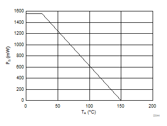
| PS | Safety input, output, or total power | θJA = 80.2°C/W, TJ = 150°C, TA = 25°C, see Figure 4 | 1558(1) | mW | ||
| TS | Maximum safety temperature | 150 | °C | |||
(1) Input, output, or the sum of input and output power must not exceed this value.
The maximum safety temperature is the maximum junction temperature specified for the device. The power dissipation and junction-to-air thermal impedance of the device installed in the application hardware determines the junction temperature. The assumed junction-to-air thermal resistance in the Thermal Information table is that of a device installed on a high-K test board for leaded surface-mount packages. The power is the recommended maximum input voltage times the current. The junction temperature is then the ambient temperature plus the power times the junction-to-air thermal resistance.
7.9 Electrical Characteristics: AMC1304x05-Q1
All minimum and maximum specifications are at TA = –40°C to 125°C, LDOIN = 4.0 V to 18.0 V, DVDD = 3.0 V to 5.5 V, AINP = –50 mV to 50 mV, AINN = 0 V, and sinc3 filter with OSR = 256, unless otherwise noted. Typical values are at TA = 25°C, CLKIN = 20 MHz, LDOIN = 15.0 V, and DVDD = 3.3 V.| PARAMETER | TEST CONDITIONS | MIN | TYP | MAX | UNIT | |
|---|---|---|---|---|---|---|
| ANALOG INPUTS | ||||||
| VClipping | Maximum differential voltage input range (AINP-AINN) |
±62.5 | mV | |||
| FSR | Specified linear full-scale range (AINP-AINN) |
–50 | 50 | mV | ||
| VCM | Operating common-mode input range | –0.032 | 1.2 | V | ||
| CID | Differential input capacitance | 2 | pF | |||
| IIB | Input bias current | Inputs shorted to AGND | –97 | –72 | –57 | μA |
| RID | Differential input resistance | 5 | kΩ | |||
| IIO | Input offset current | ±5 | nA | |||
| CMTI | Common-mode transient immunity | 15 | kV/μs | |||
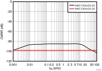
| CMRR | Common-mode rejection ratio | fIN = 0 Hz, VCM min ≤ VIN ≤ VCM max |
–98 | dB | ||
| fIN from 0.1 Hz to 50 kHz, VCM min ≤ VIN ≤ VCM max |
–85 | |||||
| BW | Input bandwidth | 800 | kHz | |||
| DC ACCURACY | ||||||
| DNL | Differential nonlinearity | Resolution: 16 bits | –0.99 | 0.99 | LSB | |
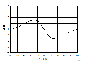
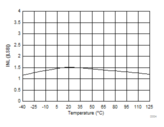
| INL | Integral nonlinearity (1) | Resolution: 16 bits | –5 | ±1.5 | 5 | LSB |
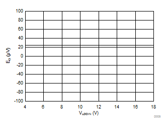
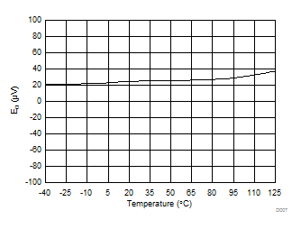
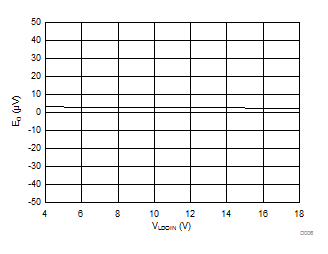
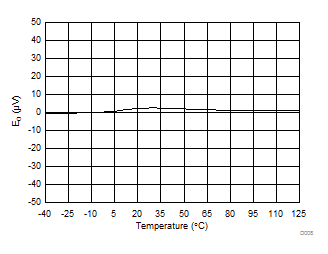
| EO | Offset error | Initial, at 25°C | –50 | ±2.5 | 50 | µV |
| TCEO | Offset error thermal drift (2) | –1.3 | 1.3 | μV/°C | ||
| EG | Gain error | Initial, at 25°C | –0.3% | –0.02% | 0.3% | |
| TCEG | Gain error thermal drift (3) | –40 | ±20 | 40 | ppm/°C | |
| PSRR | Power-supply rejection ratio | LDOIN from 4 V to 18 V, at dc | –110 | dB | ||
| LDOIN from 4 V to 18 V, from 0.1 Hz to 50 kHz | –110 | |||||
| AC ACCURACY | ||||||
| SNR | Signal-to-noise ratio | fIN = 1 kHz | 76 | 81.5 | dB | |
| SINAD | Signal-to-noise + distortion | fIN = 1 kHz | 76 | 81 | dB | |
| THD | Total harmonic distortion | fIN = 1 kHz | –90 | –81 | dB | |
| SFDR | Spurious-free dynamic range | fIN = 1 kHz | 81 | 90 | dB | |
| DIGITAL INPUTS/OUTPUTS | ||||||
| External Clock | ||||||
| fCLKIN | Input clock frequency | 5 | 20 | 20.1 | MHz | |
| DutyCLKIN | Duty cycle | 5 MHz ≤ fCLKIN ≤ 20.1 MHz | 40% | 50% | 60% | |
| CMOS Logic Family (AMC1304M05-Q1, CMOS with Schmitt Trigger) | ||||||
| IIN | Input current | DGND ≤ VIN ≤ DVDD | –1 | 1 | μA | |
| CIN | Input capacitance | 5 | pF | |||
| VIH | High-level input voltage | 0.7 × DVDD | DVDD + 0.3 | V | ||
| VIL | Low-level input voltage | –0.3 | 0.3 × DVDD | V | ||
| CLOAD | Output load capacitance | fCLKIN = 20 MHz | 30 | pF | ||
| VOH | High-level output voltage | IOH = –20 µA | DVDD – 0.1 | V | ||
| IOH = –4 mA | DVDD – 0.4 | |||||
| VOL | Low-level output voltage | IOL = 20 µA | 0.1 | V | ||
| IOL = 4 mA | 0.4 | |||||
| LVDS Logic Family (AMC1304L05-Q1)(4) | ||||||
| VT | Differential output voltage | RLOAD = 100 Ω | 250 | 350 | 450 | mV |
| VOC | Common-mode output voltage | 1.125 | 1.23 | 1.375 | V | |
| VID | Differential input voltage | 100 | 350 | 600 | mV | |
| VIC | Common-mode input voltage | VID = 100 mV | 0.05 | 1.25 | 3.25 | V |
| II | Receiver input current | DGND ≤ VIN ≤ 3.3 V | –24 | 0 | 20 | µA |
| POWER SUPPLY | ||||||
| LDOIN | LDOIN pin input voltage | 4.0 | 15.0 | 18.0 | V | |
| VCAP | VCAP pin voltage | 3.45 | V | |||
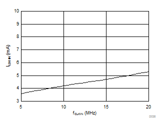
| ILDOIN | LDOIN pin input current | 5.3 | 6.5 | mA | ||
| DVDD | Controller-side supply voltage | 3.0 | 3.3 | 5.5 | V | |
| IDVDD | Controller-side supply current | LVDS, RLOAD = 100 Ω | 6.1 | 8 | mA | |
| CMOS, 3.0 V ≤ DVDD ≤ 3.6 V, CLOAD = 5 pF |
2.7 | 4.0 | ||||
| CMOS, 4.5 V ≤ DVDD ≤ 5.5 V, CLOAD = 5 pF |
3.2 | 5.5 | ||||
(1) Integral nonlinearity is defined as the maximum deviation from a straight line passing through the end-points of the ideal ADC transfer function expressed as a number of LSBs or as a percent of the specified linear full-scale range (FSR).
(2) Offset error drift is calculated using the box method, as described by the following equation:


(3) Gain error drift is calculated using the box method, as described by the following equation:


(4) For further information on electrical characteristics of LVDS interface circuits, see the TIA-644-A standard and design note Interface Circuits for TIA/EIA-644 (LVDS).
7.10 Electrical Characteristics: AMC1304x25-Q1
All minimum and maximum specifications are at TA = –40°C to 125°C, LDOIN = 4.0 V to 18.0 V, DVDD = 3.0 V to 5.5 V, AINP = –250 mV to 250 mV, AINN = 0 V, and sinc3 filter with OSR = 256, unless otherwise noted. Typical values are at TA = 25°C, CLKIN = 20 MHz, LDOIN = 15.0 V, and DVDD = 3.3 V.| PARAMETER | TEST CONDITIONS | MIN | TYP | MAX | UNIT | |
|---|---|---|---|---|---|---|
| ANALOG INPUTS | ||||||
| VClipping | Maximum differential voltage input range (AINP-AINN) |
±312.5 | mV | |||
| FSR | Specified linear full-scale range (AINP-AINN) |
–250 | 250 | mV | ||
| VCM | Operating common-mode input range | –0.16 | 1.2 | V | ||
| CID | Differential input capacitance | 1 | pF | |||
| IIB | Input bias current | Inputs shorted to AGND | –82 | –60 | –48 | μA |
| RID | Differential input resistance | 25 | kΩ | |||
| IIO | Input offset current | ±5 | nA | |||
| CMTI | Common-mode transient immunity | 15 | kV/μs | |||
| CMRR | Common-mode rejection ratio | fIN = 0 Hz, VCM min ≤ VIN ≤ VCM max |
–98 | dB | ||
| fIN from 0.1 Hz to 50 kHz, VCM min ≤ VIN ≤ VCM max |
–98 | |||||
| BW | Input bandwidth | 1000 | kHz | |||
| DC ACCURACY | ||||||
| DNL | Differential nonlinearity | Resolution: 16 bits | –0.99 | 0.99 | LSB | |
| INL | Integral nonlinearity(1) | Resolution: 16 bits | –4 | ±1.5 | 4 | LSB |
| EO | Offset error | Initial, at 25°C | –100 | ±25 | 100 | µV |
| TCEO | Offset error thermal drift(2) | –1.3 | 1.3 | μV/°C | ||
| EG | Gain error | Initial, at 25°C | –0.2% | –0.05% | 0.2% | |
| TCEG | Gain error thermal drift(3) | –40 | ±20 | 40 | ppm/°C | |
| PSRR | Power-supply rejection ratio | LDOIN from 4 V to 18 V, at dc | –110 | dB | ||
| LDOIN from 4 V to 18 V, from 0.1 Hz to 50 kHz |
–110 | |||||
| AC ACCURACY | ||||||
| SNR | Signal-to-noise ratio | fIN = 1 kHz | 82 | 85 | dB | |
| SINAD | Signal-to-noise + distortion | fIN = 1 kHz | 80 | 84 | dB | |
| THD | Total harmonic distortion | fIN = 1 kHz | –90 | –81 | dB | |
| SFDR | Spurious-free dynamic range | fIN = 1 kHz | 81 | 90 | dB | |
| DIGITAL INPUTS/OUTPUTS | ||||||
| External Clock | ||||||
| fCLKIN | Input clock frequency | 5 | 20 | 20.1 | MHz | |
| DutyCLKIN | Duty cycle | 5 MHz ≤ fCLKIN ≤ 20.1 MHz | 40% | 50% | 60% | |
| CMOS Logic Family (AMC1304M25-Q1, CMOS with Schmitt Trigger) | ||||||
| IIN | Input current | DGND ≤ VIN ≤ DVDD | –1 | 1 | μA | |
| CIN | Input capacitance | 5 | pF | |||
| VIH | High-level input voltage | 0.7 × DVDD | DVDD + 0.3 | V | ||
| VIL | Low-level input voltage | –0.3 | 0.3 × DVDD | V | ||
| CLOAD | Output load capacitance | fCLKIN = 20 MHz | 30 | pF | ||
| VOH | High-level output voltage | IOH = –20 µA | DVDD – 0.1 | V | ||
| IOH = –4 mA | DVDD – 0.4 | V | ||||
| VOL | Low-level output voltage | IOL = 20 µA | 0.1 | V | ||
| IOL = 4 mA | 0.4 | V | ||||
| LVDS Logic Family (AMC1304L25-Q1)(4) | ||||||
| VT | Differential output voltage | RLOAD = 100 Ω | 250 | 350 | 450 | mV |
| VOC | Common-mode output voltage | 1.125 | 1.23 | 1.375 | V | |
| VID | Differential input voltage | 100 | 350 | 600 | mV | |
| VIC | Common-mode input voltage | VID = 100 mV | 0.05 | 1.25 | 3.25 | V |
| II | Receiver input current | DGND ≤ VIN ≤ 3.3 V | –24 | 0 | 20 | µA |
| POWER SUPPLY | ||||||
| LDOIN | LDOIN pin input voltage | 4.0 | 15.0 | 18.0 | V | |
| VCAP | VCAP pin voltage | 3.45 | V | |||
| ILDOIN | LDOIN pin input current | 5.3 | 6.5 | mA | ||
| DVDD | Controller-side supply voltage | 3.0 | 3.3 | 5.5 | V | |
| IDVDD | Controller-side supply current | LVDS, RLOAD = 100 Ω | 6.1 | 8.0 | mA | |
| CMOS, 3.0 V ≤ DVDD ≤ 3.6 V, CLOAD = 5 pF |
2.7 | 4.0 | ||||
| CMOS, 4.5 V ≤ DVDD ≤ 5.5 V, CLOAD = 5 pF |
3.2 | 5.5 | ||||
(1) Integral nonlinearity is defined as the maximum deviation from a straight line passing through the end-points of the ideal ADC transfer function expressed as number of LSBs or as a percent of the specified linear full-scale range FSR.
(2) Offset error drift is calculated using the box method as described by the following equation:
 .
.
 .
.
(3) Gain error drift is calculated using the box method as described by the following equation:
 .
.
 .
.
(4) For further information on electrical characteristics of LVDS interface circuits, see the TIA-644-A standard and design note Interface Circuits for TIA/EIA-644 (LVDS).
7.11 Switching Characteristics
over operating free-air temperature range (unless otherwise noted)| PARAMETER | TEST CONDITIONS | MIN | TYP | MAX | UNIT | |
|---|---|---|---|---|---|---|
| tCLK | CLKIN, CLKIN_N clock period | 49.75 | 50 | 200 | ns | |
| tHIGH | CLKIN, CLKIN_N clock high time | 19.9 | 25 | 120 | ns | |
| tLOW | CLKIN, CLKIN_N clock low time | 19.9 | 25 | 120 | ns | |
| tD | Falling edge of CLKIN, CLKIN_N to DOUT, DOUT_N valid delay | 0 | 15 | ns | ||
| tISTART | Interface startup time | DVDD at 3.0 V (min) to DOUT, DOUT_N valid with LDO_IN > 4 V | 32 | 32 | CLKIN cycles | |
| tASTART | Analog startup time | LDOIN step to 4 V with DVDD ≥ 3.0 V, and 0.1 µF at VCAP pin | 1 | ms | ||
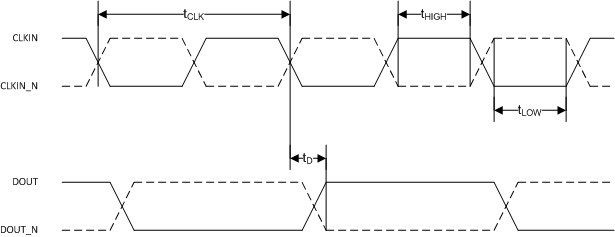 Figure 1. Digital Interface Timing
 Figure 2. Digital Interface Startup Timing
7.12 Insulation Characteristics Curves
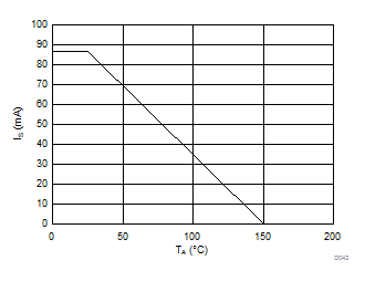
| LDOIN = 18 V (worst case) |
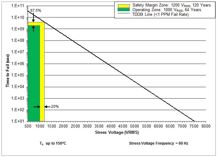
| TA up to 150°C, stress voltage frequency = 60 Hz |
7.13 Typical Characteristics
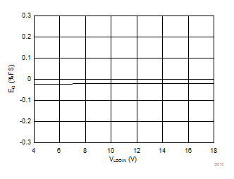
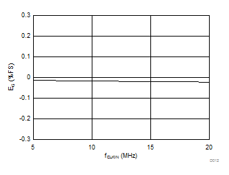
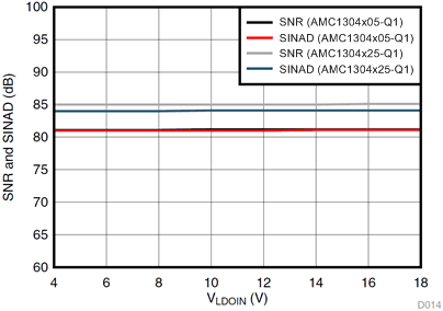
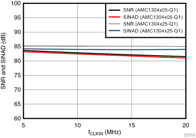
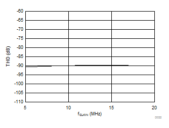
At LDOIN = 15.0 V, DVDD = 3.3 V, AINP = –50 mV to 50 mV (AMC1304x05-Q1) or –250 mV to 250 mV (AMC1304x25-Q1), AINN = 0 V, fCLKIN = 20 MHz, and sinc3 filter with OSR = 256, unless otherwise noted.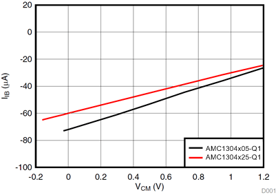
| AMC1304x25-Q1 |
| AMC1304x25-Q1 |
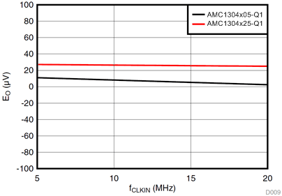
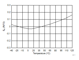
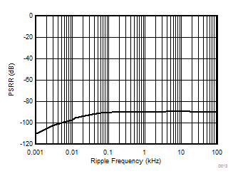
Ripple Frequency
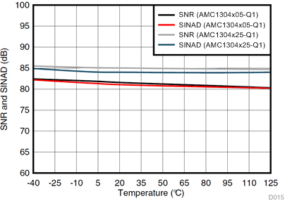
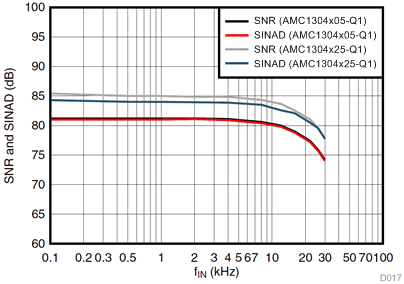
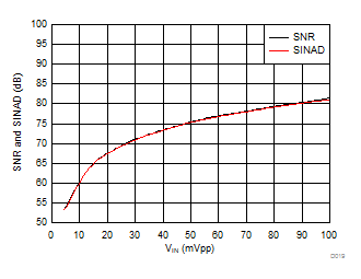
| AMC1304x05-Q1 |
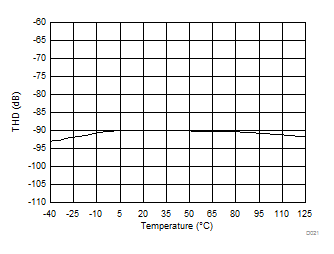
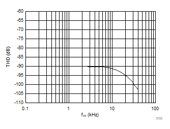
Input Signal Frequency
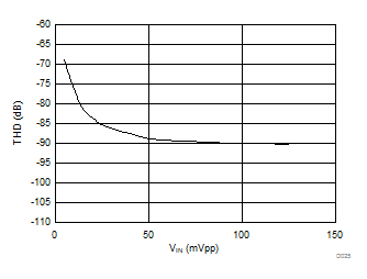
| AMC1304x05-Q1 |
Input Signal Amplitude
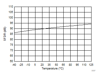
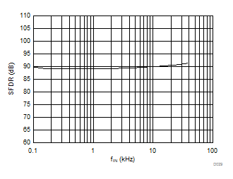
Input Signal Frequency
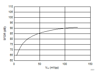
| AMC1304x05-Q1 |
Input Signal Amplitude
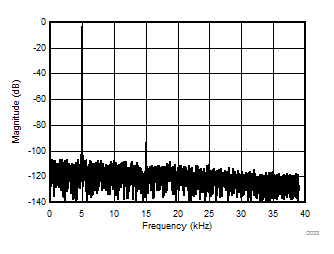
| AMC1304x05-Q1, 4096-point FFT, VIN = 100 mVPP |
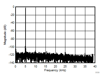
| AMC1304x25-Q1, 4096-point FFT, VIN = 500 mVPP |

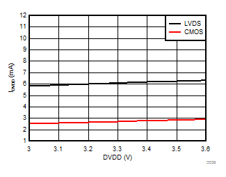
Controller-Side Supply Voltage (3.3 V, min)
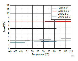
Input Signal Frequency
| AMC1304x05-Q1 |
| AMC1304x05-Q1 |
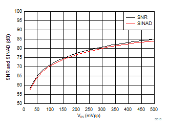
| AMC1304x25-Q1 |
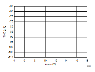
LDO Input Supply Voltage
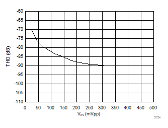
| AMC1304x25-Q1 |
Input Signal Amplitude
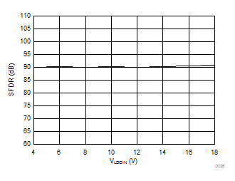
LDO Input Supply Voltage
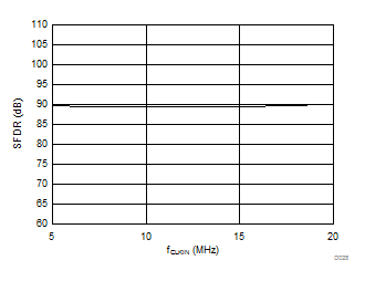
Clock Frequency
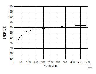
| AMC1304x25-Q1 |
Input Signal Amplitude

| AMC1304x05-Q1, 4096-point FFT, VIN = 100 mVPP |
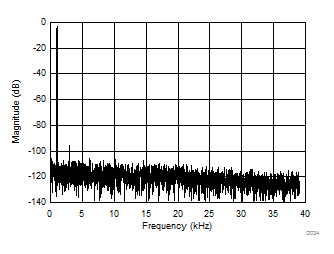
| AMC1304x25-Q1, 4096-point FFT, VIN = 500 mVPP |
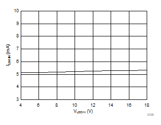
LDO Input Supply Voltage
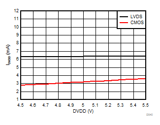
Controller-Side Supply Voltage (5 V, min)
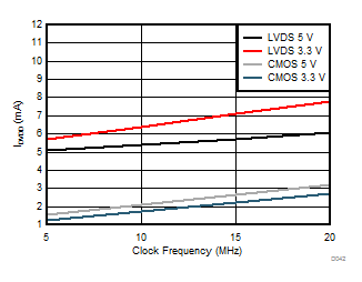
Clock Frequency