ZHCSFZ4 February 2017 AMC1304L05-Q1 , AMC1304L25-Q1 , AMC1304M05-Q1 , AMC1304M25-Q1
PRODUCTION DATA.
- 1 特性
- 2 应用
- 3 说明
- 4 修订历史记录
- 5 Device Comparison Table
- 6 Pin Configurations and Functions
-
7 Specifications
- 7.1 Absolute Maximum Ratings
- 7.2 ESD Ratings
- 7.3 Recommended Operating Conditions
- 7.4 Thermal Information
- 7.5 Power Ratings
- 7.6 Insulation Specifications
- 7.7 Safety-Related Certifications
- 7.8 Safety Limiting Values
- 7.9 Electrical Characteristics: AMC1304x05-Q1
- 7.10 Electrical Characteristics: AMC1304x25-Q1
- 7.11 Switching Characteristics
- 7.12 Insulation Characteristics Curves
- 7.13 Typical Characteristics
- 8 Detailed Description
- 9 Application and Implementation
- 10Power-Supply Recommendations
- 11Layout
- 12器件和文档支持
- 13机械、封装和可订购信息
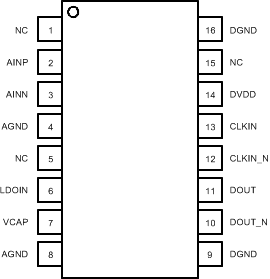
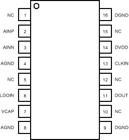
6 Pin Configurations and Functions
DW Package: LVDS Interface Versions (AMC1304Lx-Q1)
16-Pin SOIC
Top View

DW Package: CMOS Interface Versions (AMC1304Mx-Q1)
16-Pin SOIC
Top View

Pin Functions
| PIN | I/O | DESCRIPTION | ||
|---|---|---|---|---|
| NAME | NO. | |||
| AMC1304Lx-Q1 (LVDS) |
AMC1304Mx-Q1 (CMOS) |
|||
| AGND | 4 | 4 | — | This pin is internally connected to pin 8 and can be left unconnected or tied to high-side ground |
| 8 | 8 | — | High-side ground reference | |
| AINN | 3 | 3 | I | Inverting analog input |
| AINP | 2 | 2 | I | Noninverting analog input |
| CLKIN | 13 | 13 | I | Modulator clock input, 5 MHz to 20.1 MHz |
| CLKIN_N | 12 | — | I | Inverted modulator clock input |
| DGND | 9, 16 | 9, 16 | — | Controller-side ground reference |
| DOUT | 11 | 11 | O | Modulator data output |
| DOUT_N | 10 | — | O | Inverted modulator data output |
| DVDD | 14 | 14 | — | Controller-side power supply, 3.0 V to 5.5 V. See the Power-Supply Recommendations section for decoupling recommendations. |
| LDOIN | 6 | 6 | — | Low dropout regulator input, 4 V to 18 V |
| NC | 1 | 1 | — | This pin can be connected to VCAP or left unconnected |
| 5 | 5 | — | This pin can be left unconnected or tied to AGND only | |
| — | 10, 12 | — | These pins have no internal connection | |
| 15 | 15 | — | This pin can be left unconnected or tied to DVDD only | |
| VCAP | 7 | 7 | — | LDO output. See the Power-Supply Recommendations section for decoupling recommendations. |