ZHCSCZ0F June 2014 – March 2017 AMC1305L25 , AMC1305M05 , AMC1305M25
PRODUCTION DATA.
- 1 特性
- 2 应用
- 3 说明
- 4 修订历史记录
- 5 Device Comparison Table
- 6 Pin Configuration and Functions
-
7 Specifications
- 7.1 Absolute Maximum Ratings
- 7.2 ESD Ratings
- 7.3 Recommended Operating Conditions
- 7.4 Thermal Information
- 7.5 Power Ratings
- 7.6 Insulation Specifications
- 7.7 Safety-Related Certifications
- 7.8 Safety Limiting Values
- 7.9 Electrical Characteristics: AMC1305M05
- 7.10 Electrical Characteristics: AMC1305x25
- 7.11 Switching Characteristics
- 7.12 Insulation Characteristics Curves
- 7.13 Typical Characteristics
- 8 Detailed Description
- 9 Application and Implementation
- 10Power-Supply Recommendations
- 11Layout
- 12器件和文档支持
- 13机械、封装和可订购信息
10 Power-Supply Recommendations
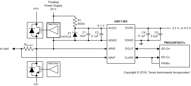
In a typical frequency inverter application, the high-side power supply (AVDD) for the device is derived from the floating power supply of the upper gate driver. For lowest cost, a Zener diode can be used to limit the voltage to 5 V ±10%. Alternatively a low-cost low-drop regulator (LDO), for example the LM317-N, can be used to minimize noise on the power supply. A low-ESR decoupling capacitor of 0.1 µF is recommended for filtering this power-supply path. Place this capacitor (C2 in Figure 58) as close as possible to the AVDD pin of the AMC1305 for best performance. If better filtering is required, an additional 10-µF capacitor can be used. The floating ground reference (AGND) is derived from the end of the shunt resistor, which is connected to the negative input (AINN) of the device. If a four-pin shunt is used, the device inputs are connected to the inner leads, while AGND is connected to one of the outer leads of the shunt.
For decoupling of the digital power supply on controller side, TI recommends using a 0.1-µF capacitor assembled as close to the DVDD pin of the AMC1305 as possible, followed by an additional capacitor in the range of 1 µF to 10 µF.
