ZHCSG26C March 2017 – Janaury 2020 AMC1306E05 , AMC1306E25 , AMC1306M05 , AMC1306M25
PRODUCTION DATA.
- 1 特性
- 2 应用
- 3 说明
- 4 修订历史记录
- 5 Device Comparison Table
- 6 Pin Configuration and Functions
-
7 Specifications
- 7.1 Absolute Maximum Ratings
- 7.2 ESD Ratings
- 7.3 Recommended Operating Conditions
- 7.4 Thermal Information
- 7.5 Power Ratings
- 7.6 Insulation Specifications
- 7.7 Safety-Related Certifications
- 7.8 Safety Limiting Values
- 7.9 Electrical Characteristics: AMC1306x05
- 7.10 Electrical Characteristics: AMC1306x25
- 7.11 Switching Characteristics
- 7.12 Insulation Characteristics Curves
- 7.13 Typical Characteristics
- 8 Detailed Description
- 9 Application and Implementation
- 10Power Supply Recommendations
- 11Layout
- 12器件和文档支持
- 13机械、封装和可订购信息
8.3.1 Analog Input
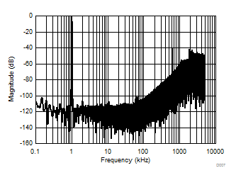
The AMC1306 incorporates front-end circuitry that contains a differential amplifier and a sampling stage, followed by a ΔΣ modulator. The gain of the differential amplifier is set by internal precision resistors to a factor of 4 for devices with a specified input voltage range of ±250 mV (this value is for the AMC1306x25), or to a factor of 20 in devices with a ±50-mV input voltage range (for the AMC1306x05), resulting in a differential input impedance of 4.9 kΩ (for the AMC1306x05) or 22 kΩ (for the AMC1306x25). For reduced offset and offset drift, the differential amplifier is chopper-stabilized with the switching frequency set at fCLKIN / 32. The switching frequency generates a spur as shown in Figure 47.

| sinc3 filter, OSR = 2, fCLKIN = 20 MHz, fIN = 1 kHz |
Consider the input impedance of the AMC1306 in designs with high-impedance signal sources that can cause degradation of gain and offset specifications. The importance of this effect, however, depends on the desired system performance. Additionally, the input bias current caused by the internal common-mode voltage at the output of the differential amplifier is dependent on the actual amplitude of the input signal; see the Isolated Voltage Sensing section for more details on reducing these effects.
There are two restrictions on the analog input signals (AINP and AINN). First, if the input voltage exceeds the range AGND – 6 V to AVDD + 0.5 V, the input current must be limited to 10 mA because the device input electrostatic discharge (ESD) diodes turn on. In addition, the linearity and noise performance of the device are ensured only when the differential analog input voltage remains within the specified linear full-scale range (FSR), that is ±250 mV (for the AMC1306x25) or ±50 mV (for the AMC1306x05), and within the specified input common-mode range.