ZHCSG26C March 2017 – Janaury 2020 AMC1306E05 , AMC1306E25 , AMC1306M05 , AMC1306M25
PRODUCTION DATA.
- 1 特性
- 2 应用
- 3 说明
- 4 修订历史记录
- 5 Device Comparison Table
- 6 Pin Configuration and Functions
-
7 Specifications
- 7.1 Absolute Maximum Ratings
- 7.2 ESD Ratings
- 7.3 Recommended Operating Conditions
- 7.4 Thermal Information
- 7.5 Power Ratings
- 7.6 Insulation Specifications
- 7.7 Safety-Related Certifications
- 7.8 Safety Limiting Values
- 7.9 Electrical Characteristics: AMC1306x05
- 7.10 Electrical Characteristics: AMC1306x25
- 7.11 Switching Characteristics
- 7.12 Insulation Characteristics Curves
- 7.13 Typical Characteristics
- 8 Detailed Description
- 9 Application and Implementation
- 10Power Supply Recommendations
- 11Layout
- 12器件和文档支持
- 13机械、封装和可订购信息
8.3.3 Isolation Channel Signal Transmission
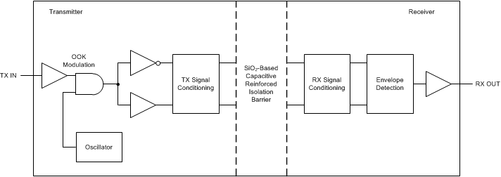
The AMC1306 device uses an on-off keying (OOK) modulation scheme to transmit the modulator output bitstream across the capacitive SiO2-based isolation barrier. The transmitter modulates the bitstream at TX IN in Figure 49 with an internally-generated, 480-MHz carrier across the isolation barrier to represent a digital one and sends a no signal to represent the digital zero. The receiver demodulates the signal after advanced signal conditioning and produces the output. The symmetrical design of each isolation channel improves the CMTI performance and reduces the radiated emissions caused by the high-frequency carrier. The block diagram of an isolation channel integrated in the AMC1306 is shown in Figure 49.
 Figure 49. Block Diagram of an Isolation Channel
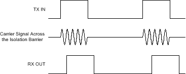
 Figure 50 shows the concept of the on-off keying scheme.
 Figure 50. OOK-Based Modulation Scheme