ZHCSG26C March 2017 – Janaury 2020 AMC1306E05 , AMC1306E25 , AMC1306M05 , AMC1306M25
PRODUCTION DATA.
- 1 特性
- 2 应用
- 3 说明
- 4 修订历史记录
- 5 Device Comparison Table
- 6 Pin Configuration and Functions
-
7 Specifications
- 7.1 Absolute Maximum Ratings
- 7.2 ESD Ratings
- 7.3 Recommended Operating Conditions
- 7.4 Thermal Information
- 7.5 Power Ratings
- 7.6 Insulation Specifications
- 7.7 Safety-Related Certifications
- 7.8 Safety Limiting Values
- 7.9 Electrical Characteristics: AMC1306x05
- 7.10 Electrical Characteristics: AMC1306x25
- 7.11 Switching Characteristics
- 7.12 Insulation Characteristics Curves
- 7.13 Typical Characteristics
- 8 Detailed Description
- 9 Application and Implementation
- 10Power Supply Recommendations
- 11Layout
- 12器件和文档支持
- 13机械、封装和可订购信息
9.1.1 Digital Filter Usage
The modulator generates a bitstream that is processed by a digital filter to obtain a digital word similar to a conversion result of a conventional analog-to-digital converter (ADC). A very simple filter, built with minimal effort and hardware, is a sinc3-type filter, as shown in Equation 2:

This filter provides the best output performance at the lowest hardware size (count of digital gates) for a second-order modulator. All the characterization in this document is also done with a sinc3 filter with an oversampling ratio (OSR) of 256 and an output word width of 16 bits.
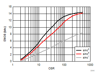
The effective number of bits (ENOB) is often used to compare the performance of ADCs and ΔΣ modulators. Figure 55 shows the ENOB of the AMC1306 with different oversampling ratios. In this document, this number is calculated from the SINAD by using Equation 3:

An example code for implementing a sinc3 filter in an FPGA is discussed in the Combining the ADS1202 with an FPGA Digital Filter for Current Measurement in Motor Control Applications application note, available for download at www.ti.com.