SBASA51 May 2020 AMC1336-Q1
PRODUCTION DATA.
- 1 Features
- 2 Applications
- 3 Description
- 4 Revision History
- 5 Pin Configuration and Functions
-
6 Specifications
- Table 1. Absolute Maximum Ratings
- Table 2. ESD Ratings
- Table 3. Recommended Operating Conditions
- Table 4. Thermal Information
- Table 5. Power Ratings
- Table 6. Insulation Specifications
- Table 7. Safety-Related Certifications
- Table 8. Safety Limiting Values
- Table 9. Electrical Characteristics
- Table 10. Switching Characteristics
- 6.1 Insulation Characteristics Curves
- 6.2 Typical Characteristics
- 7 Detailed Description
- 8 Application and Implementation
- 9 Power Supply Recommendations
- 10Layout
- 11Device and Documentation Support
- 12Mechanical, Packaging, and Orderable Information
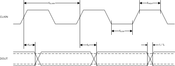
Table 10. Switching Characteristics
over operating ambient temperature range (unless otherwise noted)| PARAMETER | TEST CONDITIONS | MIN | TYP | MAX | UNIT | |
|---|---|---|---|---|---|---|
| fCLKIN | CLKIN clock frequency | 3.0 V ≤ AVDD ≤ 5.5 V | 9 | 20 | 21 | MHz |
| 4.5 V ≤ AVDD ≤ 5.5 V | 5 | 20 | 21 | |||
| CLKIN duty cycle | 40% | 50% | 60% | |||
| tH1 | DOUT hold time after rising edge of CLKIN | CLOAD = 15 pF | 3.5 | ns | ||
| tD1 | Rising edge of CLKIN to DOUT valid delay | CLOAD = 15 pF | 15 | ns | ||
| tr | DOUT rise time | 10% to 90%, 2.7 V ≤ DVDD ≤ 3.6 V, CLOAD = 15 pF | 2.5 | 6 | ns | |
| 10% to 90%, 4.5 V ≤ DVDD ≤ 5.5 V, CLOAD = 15 pF | 3.2 | 6 | ||||
| tf | DOUT fall time | 10% to 90%, 2.7 V ≤ DVDD ≤ 3.6 V, CLOAD = 15 pF | 2.2 | 6 | ns | |
| 10% to 90%, 4.5 V ≤ DVDD ≤ 5.5 V, CLOAD = 15 pF | 2.9 | 6 | ||||
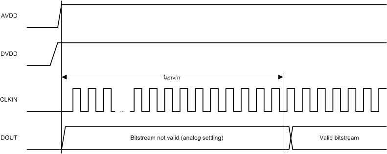
| tASTART | Analog start-up time | AVDD step to 3.0 V; 0.1%-settling, clock applied | 0.25 | ms | ||
 Figure 1. Digital Interface Timing
  Figure 2. Device Start-Up Timing