ZHCSM48A December 2020 – April 2021 AMC3306M05
PRODUCTION DATA
- 1 特性
- 2 应用
- 3 说明
- 4 Revision History
- 5 Pin Configuration and Functions
-
6 Specifications
- 6.1 Absolute Maximum Ratings
- 6.2 ESD Ratings
- 6.3 Recommended Operating Conditions
- 6.4 Thermal Information
- 6.5 Power Ratings
- 6.6 Insulation Specifications
- 6.7 Safety-Related Certifications
- 6.8 Safety Limiting Values
- 6.9 Electrical Characteristics
- 6.10 Switching Characteristics
- 6.11 Timing Diagrams
- 6.12 Insulation Characteristics Curves
- 6.13 Typical Characteristics
- 7 Detailed Description
- 8 Application and Implementation
- 9 Power Supply Recommendations
- 10Layout
- 11Device and Documentation Support
- 12Mechanical, Packaging, and Orderable Information
7.3.3 Isolation Channel Signal Transmission
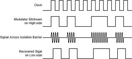
The AMC3306M05 uses an on-off keying (OOK) modulation scheme, as shown in Figure 7-3, to transmit the modulator output bitstream across the SiO2-based isolation barrier. The transmit driver (TX) shown in the Section 7.2 transmits an internally generated, high-frequency carrier across the isolation barrier to represent a digital one and does not send a signal to represent a digital zero. The nominal frequency of the carrier used inside the AMC3306M05 is 480 MHz.
The receiver (RX) on the other side of the isolation barrier recovers and demodulates the signal and produces the output. The AMC3306M05 transmission channel is optimized to achieve the highest level of common-mode transient immunity (CMTI) and lowest level of radiated emissions caused by the high-frequency carrier and RX/TX buffer switching.
 Figure 7-3 OOK-Based
Modulation Scheme