ZHCSR80A June 2009 – January 2023 AMC6821-Q1
PRODUCTION DATA
- 1 特性
- 2 应用
- 3 说明
- 4 Revision History
- 5 说明(续)
- 6 Pin Configuration and Functions
- 7 Specifications
-
8 Detailed Description
- 8.1 Functional Block Diagram
- 8.2 Feature Description
- 8.3 Device Functional Modes
- 8.4 Programming
- 8.5 Register Map
- 9 Application and Implementation
- 10Device and Documentation Support
- 11Mechanical, Packaging, and Orderable Information
6 Pin Configuration and Functions
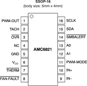
 Figure 6-1 DBQ Package16-Pin SSOPTop View
Table 6-1 Pin Functions
| PIN | I/O | DESCRIPTION | |
|---|---|---|---|
| NAME | NO. | ||
| PWM-OUT | 1 | O | Digital output, open-drain. PWM output to control fan speed. |
| TACH | 2 | I | Digital input. Fan tachometer input to measure the fan speed. |
| OVR | 3 | O | Digital output, open-drain, active low. Goes low when temperature reaches the critical shutdown threshold or remote temperature sensor failed. (See the Interrupt section for details.) |
| NC | 4 | - | Not connected. Reserved for manufacturer's testing. |
| GND | 5 | _ | System ground |
| VDD | 6 | I | Power supply, 3 V to 5 V |
| THERM | 7 | I/O | Digital input/output (open-drain). As an output, an active low output indicates the temperature over the THERM temperature limit. As an input, the pin provides an external fan control. When the pin is pulled low by external signal, the THERM-IN bit is set, and the fan is set to full-speed. |
| FAN-FAULT | 8 | O | Digital open-drain output. Goes low when a fan failure is detected. |
| IN– | 9 | I | Negative analog differential input. Connected to cathode of external temperature-sensing diode. |
| IN+ | 10 | I | Positive analog differential input. Connected to anode of external temperature-sensing diode Pentium-IV™ substrate transistor or general-purpose 2N3904 type transistor. |
| PWM-MODE | 11 | I | PWM mode selection. When tied low (GND), the high PWM frequency range (1 kHz to 40 kHz) is selected. When tied to VDD or floated, the low PWM frequency range (10 Hz to 94 Hz) is selected. Checked only on power-up or reset. |
| A1 | 12 | I | Device slave address selection pin (see the SMB Interface section for details). Checked only on power-up or reset. |
| A0 | 13 | I | Device slave address selection pin (see the SMB Interface section for details). Checked only on power-up or reset. |
| SMBALERT | 14 | O | Digital output, open-drain, SMBALERT, active low. Requires a pullup resistor (2.2 kΩ typical). |
| SDA | 15 | I/O | Bidirectional digital I/O pin, SMBus data, open-drain. Requires a pullup resistor (2.2 kΩ typical). |
| SCLK | 16 | I | Digital input, SMBus clock. Requires a pullup resistor (2.2 kΩ typical). |