ZHCSDC6D November   2014  – February 2018 AMC7836

PRODUCTION DATA.  

  1. 特性
  2. 应用
  3. 说明
  4. 修订历史记录
  5. Pin Configuration and Functions
    1.     Pin Functions
  6. Specifications
    1. 6.1  Absolute Maximum Ratings
    2. 6.2  ESD Ratings
    3. 6.3  Recommended Operating Conditions
    4. 6.4  Thermal Information
    5. 6.5  Electrical Characteristics: DAC
    6. 6.6  Electrical Characteristics: ADC and Temperature Sensor
    7. 6.7  Electrical Characteristics: General
    8. 6.8  Timing Requirements
    9. 6.9  Typical Characteristics: DAC
    10. 6.10 Typical Characteristics: ADC
    11. 6.11 Typical Characteristics: Reference
    12. 6.12 Typical Characteristics: Temperature Sensor
  7. Detailed Description
    1. 7.1 Overview
    2. 7.2 Functional Block Diagram
    3. 7.3 Feature Description
      1. 7.3.1 Digital-to-Analog Converters (DACs)
        1. 7.3.1.1 DAC Output Range and Clamp Configuration
          1. 7.3.1.1.1 Auto-Range Detection
        2. 7.3.1.2 DAC Register Structure
        3. 7.3.1.3 DAC Clear Operation
      2. 7.3.2 Analog-to-Digital Converter (ADC)
        1. 7.3.2.1 Analog Inputs
          1. 7.3.2.1.1 Bipolar Analog Inputs
          2. 7.3.2.1.2 Unipolar Analog Inputs
        2. 7.3.2.2 ADC Sequencing
        3. 7.3.2.3 ADC Synchronization
        4. 7.3.2.4 Programmable Out-of-Range Alarms
          1. 7.3.2.4.1 Unipolar Inputs Out-of-Range Alarms
          2. 7.3.2.4.2 Unipolar Inputs Out-of-Range Alarms
          3. 7.3.2.4.3 ALARMIN Alarm
          4. 7.3.2.4.4 Hysteresis
          5. 7.3.2.4.5 False-Alarm Protection
      3. 7.3.3 Internal Temperature Sensor
      4. 7.3.4 Internal Reference
      5. 7.3.5 General Purpose I/Os
    4. 7.4 Device Functional Modes
      1. 7.4.1 All-Positive DAC Range Mode
      2. 7.4.2 All-Negative DAC Range Mode
      3. 7.4.3 Mixed DAC Range Mode
    5. 7.5 Programming
    6. 7.6 Register Maps
      1. 7.6.1  Interface Configuration: Address 0x00 – 0x02
        1. 7.6.1.1 Interface Configuration 0 Register (address = 0x00) [reset = 0x30]
          1. Table 9. Interface Config 0 Register Field Descriptions (R/W)
        2. 7.6.1.2 Interface Configuration 1 Register (address = 0x01) [reset = 0x00]
          1. Table 10. Interface Config 1 Register Field Descriptions
        3. 7.6.1.3 Device Configuration Register (address = 0x02) [reset = 0x03]
          1. Table 11. Device Config Register Field Descriptions
      2. 7.6.2  Device Identification: Address 0x03 – 0x0D
        1. 7.6.2.1 Chip Type Register (address = 0x03) [reset = 0x08]
          1. Table 12. Chip Type Register Field Descriptions
        2. 7.6.2.2 Chip ID Low Byte Register (address = 0x04) [reset = 0x36]
          1. Table 13. Chip ID Low Byte Register Field Descriptions
        3. 7.6.2.3 Chip ID High Byte Register (address = 0x05) [reset = 0x0C]
          1. Table 14. Chip ID High Byte Register Field Descriptions
        4. 7.6.2.4 Version ID Register (address = 0x06) [reset = 0x00]
          1. Table 15. Version ID Register Field Descriptions
        5. 7.6.2.5 Manufacturer ID Low Byte Register (address = 0x0C) [reset = 0x51]
          1. Table 16. Manufacturer ID Low Byte Register Field Descriptions
        6. 7.6.2.6 Manufacturer ID High Byte Register (address = 0x0D) [reset = 0x04]
          1. Table 17. Manufacturer ID High Byte Register Field Descriptions
      3. 7.6.3  Register Update (Buffered Registers): Address 0x0F
        1. 7.6.3.1 Register Update Register (address = 0x0F) [reset = 0x00]
          1. Table 18. Register Update Register Field Descriptions
      4. 7.6.4  General Device Configuration: Address 0x10 through 0x17
        1. 7.6.4.1 ADC Configuration Register (address = 0x10) [reset = 0x00]
          1. Table 19. ADC Configuration Register Field Descriptions
        2. 7.6.4.2 False Alarm Configuration Register (address = 0x11) [reset = 0x70]
          1. Table 21. False Alarm Configuration Register Field Descriptions
        3. 7.6.4.3 GPIO Configuration Register (address = 0x12) [reset = 0x00]
          1. Table 24. GPIO Configuration Register Field Descriptions
        4. 7.6.4.4 ADC MUX Configuration 0 Register (address = 0x13) [reset = 0x00]
          1. Table 25. ADC MUX Configuration 0 Register Field Descriptions
        5. 7.6.4.5 ADC MUX Configuration 1 Register (address = 0x14) [reset = 0x00]
          1. Table 26. ADC MUX Configuration 1 Register Field Descriptions
        6. 7.6.4.6 ADC MUX Configuration 2 Register (address = 0x15) [reset = 0x00]
          1. Table 27. ADC MUX Configuration 2 Register Field Descriptions
        7. 7.6.4.7 DAC Clear Enable 0 Register (address = 0x18) [reset = 0x00]
          1. Table 28. DAC Clear Enable 0 Register Field Descriptions
        8. 7.6.4.8 DAC Clear Enable 1 Register (address = 0x19) [reset = 0x00]
          1. Table 29. DAC Clear Enable 1 Register Field Descriptions
      5. 7.6.5  DAC Clear and ALARMOUT Source Select: Address 0x1A through 0x1D
        1. 7.6.5.1 DAC Clear Source 0 Register (address = 0x1A) [reset = 0x00]
          1. Table 30. DAC Clear Source 0 Register Field Descriptions
        2. 7.6.5.2 DAC Clear Source 1 Register (address = 0x1B) [reset = 0x00]
          1. Table 31. DAC Clear Source 1 Register Field Descriptions
        3. 7.6.5.3 ALARMOUT Source 0 Register (address = 0x1c) [reset = 0x00]
          1. Table 32. ALARMOUT Source 0 Register Field Descriptions
        4. 7.6.5.4 ALARMOUT Source 1 Register (address = 0x1D) [reset = 0x00]
          1. Table 33. ALARMOUT Source 1 Register Field Descriptions
      6. 7.6.6  DAC Range: Address 0x1E
        1. 7.6.6.1 DAC Range Register (address = 0x1E) [reset = 0x00]
          1. Table 34. DAC Range Register Field Descriptions
        2. 7.6.6.2 DAC Range 1 Register (address = 0x1F) [reset = 0x00]
          1. Table 36. DAC Range 1 Register Field Descriptions
      7. 7.6.7  ADC and Temperature Data: Address 0x20 through 0x4B
        1. 7.6.7.1 ADCn-Data (Low Byte) Register (address = 0x20 through 0x49) [reset = 0x00]
          1. Table 37. ADCn-Data (Low Byte) Register Field Descriptions
        2. 7.6.7.2 ADCn-Data (High Byte) Register (address = 0x20 through 0x49) [reset = 0x00]
          1. Table 38. ADCn-Data (High Byte) Register Field Descriptions
        3. 7.6.7.3 Temperature Data (Low Byte) Register (address = 0x4A) [reset = 0x00]
          1. Table 39. Temperature Data (Low Byte) Register Field Descriptions
        4. 7.6.7.4 Temperature Data (High Byte) Register (address = 0x4B) [reset = 0x00]
          1. Table 40. Temperature Data (High Byte) Register Field Descriptions
      8. 7.6.8  DAC Data: Address 0x50 through 0x6F
        1. 7.6.8.1 DACn-Data (Low Byte) Register (address = 0x50 through 0x6F) [reset = 0x00]
          1. Table 41. DACn-Data (Low Byte) Register Field Descriptions
        2. 7.6.8.2 DACn Data (High Byte) Register (address = 0x50 through 0x6F) [reset = 0x00]
          1. Table 42. DACn Data (High Byte) Register Field Descriptions
      9. 7.6.9  Status Registers: Address 0x70 through 0x72
        1. 7.6.9.1 Alarm Status 0 Register (address = 0x70) [reset = 0x00]
          1. Table 43. Alarm Status 0 Register Field Descriptions
        2. 7.6.9.2 Alarm Status 1 Register (address = 0x71) [reset = 0x00]
          1. Table 44. Alarm Status 1 Register Field Descriptions
        3. 7.6.9.3 General Status Register (address = 0x72) [reset = 0x0C]
          1. Table 45. General Status Register Field Descriptions
      10. 7.6.10 GPIO: Address 0x7A
        1. 7.6.10.1 GPIO Register (address = 0x7A) [reset = 0xFF]
          1. Table 46. GPIO Register Field Descriptions
      11. 7.6.11 Out-Of-Range ADC Thresholds: Address 0x80 through 0x93
        1. 7.6.11.1 ADCn-Upper-Thresh (Low Byte) Register (address = 0x80 through 0x93) [reset = 0xFF]
          1. Table 47. ADCn-Upper-Thresh (Low Byte) Register Field Descriptions
        2. 7.6.11.2 ADCn-Upper-Thresh (High Byte) Register (address = 0x80 through 0x93) [reset = 0x0F]
          1. Table 48. ADCn-Upper-Thresh (High Byte) Register Field Descriptions
        3. 7.6.11.3 ADCn-Lower-Thresh (Low Byte) Register (address = 0x80 through 0x93) [reset = 0x00]
          1. Table 49. ADCn-Lower-Thresh (Low Byte) Register Field Descriptions
        4. 7.6.11.4 ADCn-Lower-Thresh (High Byte) Register (address = 0x80 through 0x93) [reset = 0x00]
          1. Table 50. ADCn-Lower-Thresh (High Byte) Register Field Descriptions Field Descriptions
        5. 7.6.11.5 LT-Upper-Thresh (Low Byte) Register (address = 0x94) [reset = 0xFF]
          1. Table 51. LT-Upper-Thresh (Low Byte) Register Field Descriptions
        6. 7.6.11.6 LT-Upper-Thresh (High Byte) Register (address = 0x95) [reset = 0x07]
          1. Table 52. LT-Upper-Thresh (High Byte) Register Field Descriptions
        7. 7.6.11.7 LT-Lower-Thresh (Low Byte) Register (address = 0x96) [reset = 0x00]
          1. Table 53. LT-Lower-Thresh (Low Byte) Register Field Descriptions
        8. 7.6.11.8 LT-Lower-Thresh (High Byte) Register (address = 0x97) [reset = 0x08]
          1. Table 54. LT-Lower-Thresh (High Byte) Register Field Descriptions
      12. 7.6.12 Alarm Hysteresis Configuration: Address 0xA0 and 0xA5
        1. 7.6.12.1 ADCn-Hysteresis Register (address = 0xA0 through 0xA4) [reset = 0x08]
          1. Table 55. ADCn-Hysteresis Register Field Descriptions
        2. 7.6.12.2 LT-Hysteresis Register (address = 0xA5) [reset = 0x08]
          1. Table 56. LT-Hysteresis Register Field Descriptions
      13. 7.6.13 Clear and Power-Down Registers: Address 0xB0 through 0XB4
        1. 7.6.13.1 DAC Clear 0 Register (address = 0xB0) [reset = 0x00]
          1. Table 57. DAC Clear 0 Register Field Descriptions
        2. 7.6.13.2 DAC Clear 1 Register (address = 0xB1) [reset = 0x00]
          1. Table 58. DAC Clear 1 Register Field Descriptions
        3. 7.6.13.3 Power-Down 0 Register (address = 0xB2) [reset = 0x00]
          1. Table 59. Power-Down 0 Register Field Descriptions
        4. 7.6.13.4 Power-Down 1 Register (address = 0xB3) [reset = 0x00]
          1. Table 60. Power-Down 1 Register Field Descriptions
        5. 7.6.13.5 Power-Down 2 Register (address = 0xB4) [reset = 0x00]
          1. Table 61. Power-Down 2 Register Field Descriptions
      14. 7.6.14 ADC Trigger: Address 0xC0
        1. 7.6.14.1 ADC Trigger Register (address = 0xC0) [reset = 0x00]
          1. Table 62. ADC Trigger Register Field Descriptions
  8. Application and Implementation
    1. 8.1 Application Information
      1. 8.1.1 Temperature Sensing Applications
      2. 8.1.2 Current Sensing Applications
    2. 8.2 Typical Application
      1. 8.2.1 Design Requirements
      2. 8.2.2 Detailed Design Procedure
        1. 8.2.2.1 ADC Input Conditioning
        2. 8.2.2.2 DAC Output Range Selection
      3. 8.2.3 Application Curves
  9. Power Supply Recommendations
    1. 9.1 Device Reset Options
      1. 9.1.1 Power-on-Reset (POR)
      2. 9.1.2 Hardware Reset
        1. 9.1.2.1 Software Reset
  10. 10Layout
    1. 10.1 Layout Guidelines
    2. 10.2 Layout Example
  11. 11器件和文档支持
    1. 11.1 文档支持
      1. 11.1.1 相关文档
    2. 11.2 接收文档更新通知
    3. 11.3 社区资源
    4. 11.4 商标
    5. 11.5 静电放电警告
    6. 11.6 Glossary
  12. 12机械、封装和可订购信息

封装选项

机械数据 (封装 | 引脚)
散热焊盘机械数据 (封装 | 引脚)
订购信息

Programmable Out-of-Range Alarms

The AMC7836 device is capable of continuously analyzing the five external unipolar inputs and internal temperature sensor conversion results for normal operation.

Normal operation is established through the lower and upper threshold registers (address 0x80 through 0x97). When any of the monitored inputs is out of the specified range, an alarm event is issued and the global alarm bit, GALR in the general status register (0x72), is set (see Figure 54). Use the alarm status registers (0x70 through 0x71) to determine the source of the alarm event.
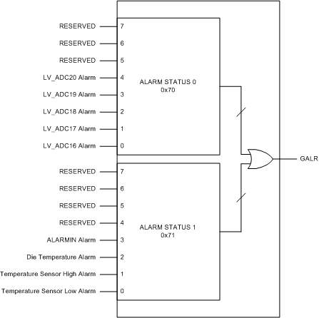
AMC7836 alarm_register_slas986.gifFigure 54. Alarm Status Register

The ALARM-LATCH-DIS bit in the ALARMOUT source 1 register (address 0x1D) sets the latching behavior for all alarms (except for the ALARMIN alarm which is always unlatched). When the ALARM-LATCH-DIS bit is cleared to 0 the alarm bits in the alarm status registers are latched. The alarm bits are referred to as being latched because they remain set until read by software. This design ensures that out-of-limit events cannot be missed if the software is polling the device periodically. All bits are cleared when reading the alarm status registers, and all bits are reasserted if the out-of limit condition still exists on the next monitoring cycle, unless otherwise noted. When the ALARM-LATCH-DIS bit is set to 1, the alarm bits are not latched. The alarm bits in the alarm status registers are set to 0 when the error condition subsides, regardless of whether the bit is read or not.

All of the alarms can be set to activate the ALARMOUT pin. To enable this functionality, the GPIO1/ALARMOUT pin must be configured accordingly in the GPIO configuration register (address 0x12). The ALARMOUT pin works as an interrupt to the host so that it can query the alarm status registers to determine the alarm source. Any alarm event can activate the pin as long as the alarm is not masked in the ALARMOUT source registers (address 0x1C through 0x1D). When an alarm event is masked, the occurrence of the event sets the corresponding status bit in the alarm status registers, but does not activate the ALARMOUT pin.