ZHCSFJ7C August 2016 – December 2018 AMIC110
PRODUCTION DATA.
- 1器件概述
- 2修订历史记录
- 3Device Comparison
- 4Terminal Configuration and Functions
-
5Specifications
- 5.1 Absolute Maximum Ratings
- 5.2 ESD Ratings
- 5.3 Power-On Hours (POH)
- 5.4 Operating Performance Points (OPPs)
- 5.5 Recommended Operating Conditions
- 5.6 Power Consumption Summary
- 5.7 DC Electrical Characteristics
- 5.8 Thermal Resistance Characteristics for ZCE and ZCZ Packages
- 5.9 External Capacitors
- 5.10 Touch Screen Controller and Analog-to-Digital Subsystem Electrical Parameters
-
6Power and Clocking
- 6.1 Power Supplies
- 6.2
Clock Specifications
- 6.2.1 Input Clock Specifications
- 6.2.2 Input Clock Requirements
- 6.2.3 Output Clock Specifications
- 6.2.4 Output Clock Characteristics
-
7Peripheral Information and Timings
- 7.1 Parameter Information
- 7.2 Recommended Clock and Control Signal Transition Behavior
- 7.3 OPP50 Support
- 7.4 Controller Area Network (CAN)
- 7.5 DMTimer
- 7.6
Ethernet Media Access Controller (EMAC) and Switch
- 7.6.1
EMAC and Switch Electrical Data and Timing
- Table 7-7 EMAC and Switch Timing Conditions
- 7.6.1.1 EMAC/Switch MDIO Electrical Data and Timing
- 7.6.1.2
EMAC and Switch MII Electrical Data and Timing
- Table 7-11 Timing Requirements for GMII[x]_RXCLK - MII Mode
- Table 7-12 Timing Requirements for GMII[x]_TXCLK - MII Mode
- Table 7-13 Timing Requirements for GMII[x]_RXD[3:0], GMII[x]_RXDV, and GMII[x]_RXER - MII Mode
- Table 7-14 Switching Characteristics for GMII[x]_TXD[3:0], and GMII[x]_TXEN - MII Mode
- 7.6.1.3 EMAC and Switch RMII Electrical Data and Timing
- 7.6.1.4
EMAC and Switch RGMII Electrical Data and Timing
- Table 7-18 Timing Requirements for RGMII[x]_RCLK - RGMII Mode
- Table 7-19 Timing Requirements for RGMII[x]_RD[3:0], and RGMII[x]_RCTL - RGMII Mode
- Table 7-20 Switching Characteristics for RGMII[x]_TCLK - RGMII Mode
- Table 7-21 Switching Characteristics for RGMII[x]_TD[3:0], and RGMII[x]_TCTL - RGMII Mode
- 7.6.1
EMAC and Switch Electrical Data and Timing
- 7.7
External Memory Interfaces
- 7.7.1 General-Purpose Memory Controller (GPMC)
- 7.7.2
mDDR(LPDDR), DDR2, DDR3, DDR3L Memory Interface
- 7.7.2.1
mDDR (LPDDR) Routing Guidelines
- 7.7.2.1.1 Board Designs
- 7.7.2.1.2 LPDDR Interface
- 7.7.2.1.3 LPDDR CK and ADDR_CTRL Routing
- 7.7.2.2
DDR2 Routing Guidelines
- 7.7.2.2.1 Board Designs
- 7.7.2.2.2
DDR2 Interface
- 7.7.2.2.2.1 DDR2 Interface Schematic
- 7.7.2.2.2.2 Compatible JEDEC DDR2 Devices
- 7.7.2.2.2.3 PCB Stackup
- 7.7.2.2.2.4 Placement
- 7.7.2.2.2.5 DDR2 Keepout Region
- 7.7.2.2.2.6 Bulk Bypass Capacitors
- 7.7.2.2.2.7 High-Speed (HS) Bypass Capacitors
- 7.7.2.2.2.8 Net Classes
- 7.7.2.2.2.9 DDR2 Signal Termination
- 7.7.2.2.2.10 DDR_VREF Routing
- 7.7.2.2.3 DDR2 CK and ADDR_CTRL Routing
- 7.7.2.3
DDR3 and DDR3L Routing Guidelines
- 7.7.2.3.1 Board Designs
- 7.7.2.3.2 DDR3 Device Combinations
- 7.7.2.3.3
DDR3 Interface
- 7.7.2.3.3.1 DDR3 Interface Schematic
- 7.7.2.3.3.2 Compatible JEDEC DDR3 Devices
- 7.7.2.3.3.3 PCB Stackup
- 7.7.2.3.3.4 Placement
- 7.7.2.3.3.5 DDR3 Keepout Region
- 7.7.2.3.3.6 Bulk Bypass Capacitors
- 7.7.2.3.3.7 High-Speed Bypass Capacitors
- 7.7.2.3.3.8 Net Classes
- 7.7.2.3.3.9 DDR3 Signal Termination
- 7.7.2.3.3.10 DDR_VREF Routing
- 7.7.2.3.3.11 VTT
- 7.7.2.3.4 DDR3 CK and ADDR_CTRL Topologies and Routing Definition
- 7.7.2.3.5 Data Topologies and Routing Definition
- 7.7.2.3.6 Routing Specification
- 7.7.2.1
mDDR (LPDDR) Routing Guidelines
- 7.8 I2C
- 7.9 JTAG Electrical Data and Timing
- 7.10 LCD Controller (LCDC)
- 7.11 Multichannel Audio Serial Port (McASP)
- 7.12 Multichannel Serial Port Interface (McSPI)
- 7.13
Multimedia Card (MMC) Interface
- 7.13.1
MMC Electrical Data and Timing
- Table 7-85 MMC Timing Conditions
- Table 7-86 Timing Requirements for MMC[x]_CMD and MMC[x]_DAT[7:0]
- Table 7-87 Switching Characteristics for MMC[x]_CLK
- Table 7-88 Switching Characteristics for MMC[x]_CMD and MMC[x]_DAT[7:0]—Standard Mode
- Table 7-89 Switching Characteristics for MMC[x]_CMD and MMC[x]_DAT[7:0]—High-Speed Mode
- 7.13.1
MMC Electrical Data and Timing
- 7.14
Programmable Real-Time Unit Subsystem and Industrial Communication Subsystem (PRU-ICSS)
- 7.14.1 Programmable Real-Time Unit (PRU-ICSS PRU)
- 7.14.2
PRU-ICSS EtherCAT (PRU-ICSS ECAT)
- Table 7-96 PRU-ICSS ECAT Timing Conditions
- 7.14.2.1
PRU-ICSS ECAT Electrical Data and Timing
- Table 7-97 PRU-ICSS ECAT Timing Requirements – Input Validated With LATCH_IN
- Table 7-98 PRU-ICSS ECAT Timing Requirements – Input Validated With SYNCx
- Table 7-99 PRU-ICSS ECAT Timing Requirements – Input Validated With Start of Frame (SOF)
- Table 7-100 PRU-ICSS ECAT Timing Requirements - LATCHx_IN
- Table 7-101 PRU-ICSS ECAT Switching Requirements - Digital I/Os
- 7.14.3 PRU-ICSS MII_RT and Switch
- 7.14.4 PRU-ICSS Universal Asynchronous Receiver Transmitter (PRU-ICSS UART)
- 7.15 Universal Asynchronous Receiver Transmitter (UART)
- 8Device and Documentation Support
- 9Mechanical, Packaging, and Orderable Information
6.1.1 Power Supply Slew Rate Requirement
To maintain the safe operating range of the internal ESD protection devices, TI recommends limiting the maximum slew rate for powering on the supplies to be less than 1.0E +5 V/s. For instance, as shown in Figure 6-1, TI recommends a value greater than 18 µs for the supply ramp slew for a 1.8-V supply.
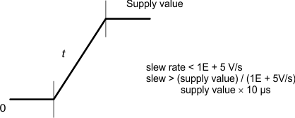 Figure 6-1 Power Supply Slew and Slew Rate
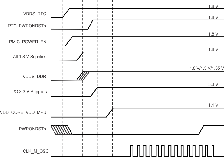
A. RTC_PWRONRSTn should be asserted for at least 1 ms to provide enough time for the internal RTC LDO output to reach a valid level before RTC reset is released.
B. When using the ZCZ package option, VDD_MPU and VDD_CORE power inputs may be powered from the same source if the application only uses operating performance points (OPPs) that define a common power supply voltage for VDD_MPU and VDD_CORE. The ZCE package option has the VDD_MPU domain merged with the VDD_CORE domain.
C. If a USB port is not used, the respective VDDA1P8V_USB terminal may be connected to any 1.8-V power supply and the respective VDDA3P3V_USB terminal may be connected to any 3.3-V power supply. If the system does not have a 3.3-V power supply, the VDDA3P3V_USB terminal may be connected to ground.
D. If the system uses mDDR or DDR2 memory devices, VDDS_DDR can be ramped simultaneously with the other 1.8-V I/O power supplies.
E. VDDS_RTC can be ramped independent of other power supplies if PMIC_POWER_EN functionality is not required. If VDDS_RTC is ramped after VDD_CORE, there might be a small amount of additional leakage current on VDD_CORE. The power sequence shown provides the lowest leakage option.
F. To configure VDDSHVx [1-6] as 1.8 V, power up the respective VDDSHVx [1-6] to 1.8 V following the recommended sequence. To configure VDDSHVx [1-6] as 3.3 V, power up the respective VDDSHVx [1-6] to 3.3 V following the recommended sequence.
G. If all the 1.8-V supplies are not sourced from the same power supply, it is required to power up VDDS before other 1.8-V supplies. Further, it is also recommended to source VDDS and VDDSHvx [x = 1-6] when configured as 1.8V from the same power supply.
Figure 6-2 Preferred Power-Supply Sequencing With Dual-Voltage I/Os Configured as 3.3 V 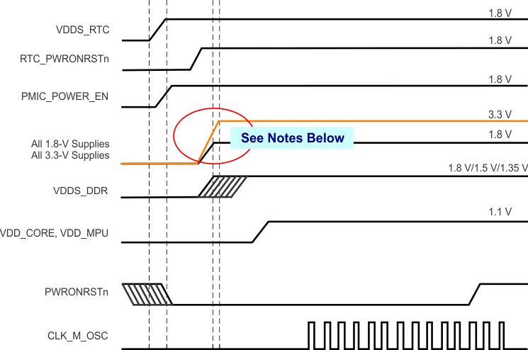
A. RTC_PWRONRSTn should be asserted for at least 1 ms to provide enough time for the internal RTC LDO output to reach a valid level before RTC reset is released.
B. The 3.3-V I/O power supplies may be ramped simultaneously with the 1.8-V I/O power supplies if the voltage sourced by any 3.3-V power supplies does not exceed the voltage sourced by any 1.8-V power supply by more than 2 V. Serious reliability issues may occur if the system power supply design allows any 3.3-V I/O power supplies to exceed any 1.8-V I/O power supplies by more than 2 V.
C. When using the ZCZ package option, VDD_MPU and VDD_CORE power inputs may be powered from the same source if the application only uses operating performance points (OPPs) that define a common power supply voltage for VDD_MPU and VDD_CORE. The ZCE package option has the VDD_MPU domain merged with the VDD_CORE domain.
D. If a USB port is not used, the respective VDDA1P8V_USB terminal may be connected to any 1.8-V power supply and the respective VDDA3P3V_USB terminal may be connected to any 3.3-V power supply. If the system does not have a 3.3-V power supply, the VDDA3P3V_USB terminal may be connected to ground.
E. If the system uses mDDR or DDR2 memory devices, VDDS_DDR can be ramped simultaneously with the other 1.8-V I/O power supplies.
F. VDDS_RTC can be ramped independent of other power supplies if PMIC_POWER_EN functionality is not required. If VDDS_RTC is ramped after VDD_CORE, there might be a small amount of additional leakage current on VDD_CORE. The power sequence shown provides the lowest leakage option.
G. To configure VDDSHVx [1-6] as 1.8 V, power up the respective VDDSHVx [1-6] to 1.8 V following the recommended sequence. To configure VDDSHVx [1-6] as 3.3 V, power up the respective VDDSHVx [1-6] to 3.3 V following the recommended sequence.
H. If all the 1.8-V supplies are not sourced from the same power supply, it is required to power up VDDS before other 1.8-V supplies. Further, it is also recommended to source VDDS and VDDSHvx [x = 1-6] when configured as 1.8V from the same power supply.
Figure 6-3 Alternate Power-Supply Sequencing With Dual-Voltage I/Os Configured as 3.3 V 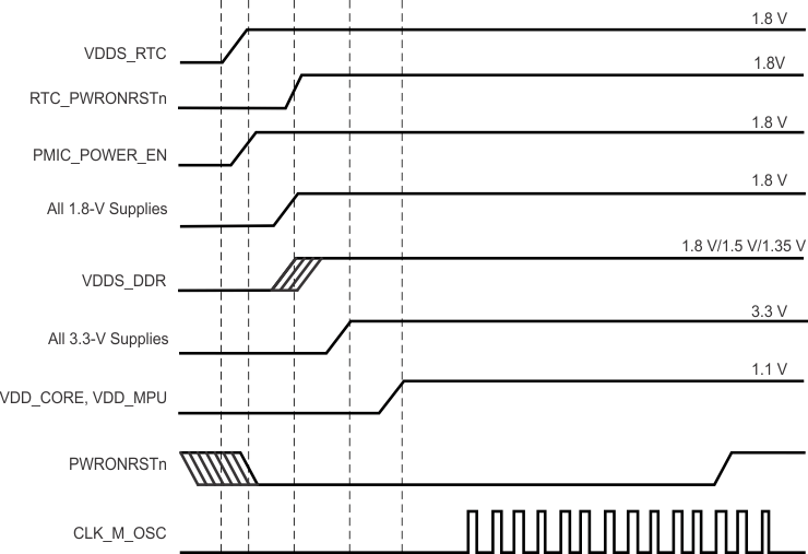
A. RTC_PWRONRSTn should be asserted for at least 1 ms to provide enough time for the internal RTC LDO output to reach a valid level before RTC reset is released.
B. When using the ZCZ package option, VDD_MPU and VDD_CORE power inputs may be powered from the same source if the application only uses operating performance points (OPPs) that define a common power supply voltage for VDD_MPU and VDD_CORE. The ZCE package option has the VDD_MPU domain merged with the VDD_CORE domain.
C. If a USB port is not used, the respective VDDA1P8V_USB terminal may be connected to any 1.8-V power supply and the respective VDDA3P3V_USB terminal may be connected to any 3.3-V power supply. If the system does not have a 3.3-V power supply, the VDDA3P3V_USB terminal may be connected to ground.
D. If the system uses mDDR or DDR2 memory devices, VDDS_DDR can be ramped simultaneously with the other 1.8-V I/O power supplies.
E. VDDS_RTC can be ramped independent of other power supplies if PMIC_POWER_EN functionality is not required. If VDDS_RTC is ramped after VDD_CORE, there might be a small amount of additional leakage current on VDD_CORE. The power sequence shown provides the lowest leakage option.
F. To configure VDDSHVx [1-6] as 1.8 V, power up the respective VDDSHVx [1-6] to 1.8 V following the recommended sequence. To configure VDDSHVx [1-6] as 3.3 V, power up the respective VDDSHVx [1-6] to 3.3 V following the recommended sequence.
G. If all the 1.8-V supplies are not sourced from the same power supply, it is required to power up VDDS before other 1.8-V supplies. Further, it is also recommended to source VDDS and VDDSHvx [x = 1-6] when configured as 1.8V from the same power supply.
Figure 6-4 Power-Supply Sequencing With Dual-Voltage I/Os Configured as 1.8 V 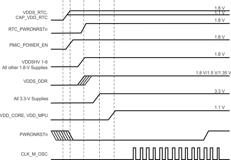
A. RTC_PWRONRSTn should be asserted for at least 1 ms to provide enough time for the internal RTC LDO output to reach a valid level before RTC reset is released.
B. The CAP_VDD_RTC terminal operates as an input to the RTC core voltage domain when the internal RTC LDO is disabled by connecting the RTC_KALDO_ENn terminal to VDDS_RTC. If the internal RTC LDO is disabled, CAP_VDD_RTC should be sourced from an external 1.1-V power supply.
C. When using the ZCZ package option, VDD_MPU and VDD_CORE power inputs may be powered from the same source if the application only uses operating performance points (OPPs) that define a common power supply voltage for VDD_MPU and VDD_CORE. The ZCE package option has the VDD_MPU domain merged with the VDD_CORE domain.
D. If a USB port is not used, the respective VDDA1P8V_USB terminal may be connected to any 1.8-V power supply and the respective VDDA3P3V_USB terminal may be connected to any 3.3-V power supply. If the system does not have a 3.3-V power supply, the VDDA3P3V_USB terminal may be connected to ground.
E. If the system uses mDDR or DDR2 memory devices, VDDS_DDR can be ramped simultaneously with the other 1.8-V I/O power supplies.
F. VDDS_RTC should be ramped at the same time or before CAP_VDD_RTC, but these power inputs can be ramped independent of other power supplies if PMIC_POWER_EN functionality is not required. If CAP_VDD_RTC is ramped after VDD_CORE, there might be a small amount of additional leakage current on VDD_CORE. The power sequence shown provides the lowest leakage option.
G. To configure VDDSHVx [1-6] as 1.8 V, power up the respective VDDSHVx [1-6] to 1.8 V following the recommended sequence. To configure VDDSHVx [1-6] as 3.3 V, power up the respective VDDSHVx [1-6] to 3.3 V following the recommended sequence.
H. If all the 1.8-V supplies are not sourced from the same power supply, it is required to power up VDDS before other 1.8-V supplies. Further, it is also recommended to source VDDS and VDDSHvx [x = 1-6] when configured as 1.8V from the same power supply.
Figure 6-5 Power-Supply Sequencing With Internal RTC LDO Disabled 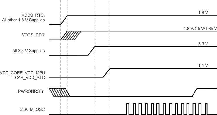
A. CAP_VDD_RTC terminal operates as an input to the RTC core voltage domain when the internal RTC LDO is disabled by connecting the RTC_KALDO_ENn terminal to VDDS_RTC. If the internal RTC LDO is disabled, CAP_VDD_RTC should be sourced from an external 1.1-V power supply. The PMIC_POWER_EN output cannot be used when the RTC is disabled.
B. When using the ZCZ package option, VDD_MPU and VDD_CORE power inputs may be powered from the same source if the application only uses operating performance points (OPPs) that define a common power supply voltage for VDD_MPU and VDD_CORE. The ZCE package option has the VDD_MPU domain merged with the VDD_CORE domain.
C. If a USB port is not used, the respective VDDA1P8V_USB terminal may be connected to any 1.8-V power supply and the respective VDDA3P3V_USB terminal may be connected to any 3.3-V power supply. If the system does not have a 3.3-V power supply, the VDDA3P3V_USB terminal may be connected to ground.
D. If the system uses mDDR or DDR2 memory devices, VDDS_DDR can be ramped simultaneously with the other 1.8-V I/O power supplies.
E. VDDS_RTC should be ramped at the same time or before CAP_VDD_RTC, but these power inputs can be ramped independent of other power supplies if PMIC_POWER_EN functionality is not required. If CAP_VDD_RTC is ramped after VDD_CORE, there might be a small amount of additional leakage current on VDD_CORE. The power sequence shown provides the lowest leakage option.
F. To configure VDDSHVx [1-6] as 1.8 V, power up the respective VDDSHVx [1-6] to 1.8 V following the recommended sequence. To configure VDDSHVx [1-6] as 3.3 V, power up the respective VDDSHVx [1-6] to 3.3 V following the recommended sequence.
G. If all the 1.8-V supplies are not sourced from the same power supply, it is required to power up VDDS before other 1.8-V supplies. Further, it is also recommended to source VDDS and VDDSHvx [x = 1-6] when configured as 1.8V from the same power supply.
Figure 6-6 Power-Supply Sequencing With RTC Feature Disabled