ZHCSDN9A March 2015 – April 2015 ATL431 , ATL432
PRODUCTION DATA.
- 1 特性
- 2 应用
- 3 说明
- 4 简化电路原理图
- 5 修订历史记录
- 6 Pin Configuration and Functions
- 7 Specifications
- 8 Parameter Measurement Information
- 9 Detailed Description
- 10Applications and Implementation
- 11Power Supply Recommendations
- 12Layout
- 13器件和文档支持
- 14机械、封装和可订购信息
10 Applications and Implementation
NOTE
Information in the following applications sections is not part of the TI component specification, and TI does not warrant its accuracy or completeness. TI’s customers are responsible for determining suitability of components for their purposes. Customers should validate and test their design implementation to confirm system functionality.
10.1 Application Information
Figure 30 shows the ATL43x used in a 24-V isolated flyback supply. The output of the regulator, plus the forward voltage drop of the optocoupler LED (2.5 + 0.7 = 3.2 V), determine the minimum voltage that can be regulated in an isolated supply configuration. Regulated voltage as low as 5.0 Vdc is possible in the topology shown in Figure 30.
The 431 family of devices are prevalent in these applications, being designers go to choice for secondary side regulation. Due to this prevalence, this section will further go on to explain operation and design in both states of ATL43x that this application will see, open loop (Comparator + Vref) & closed loop (Shunt Regulator).
ATL43x's key benefit in isolated supplies is the no load power savings gained by the > 20x decrease in IKmin from TL431. More information about this and other benefits can be found in the application note Designing with the "Advanced" TL431, ATL431SLVA685. Further information about system stability and using a ATL43x device for compensation can be found in the application note Compensation Design With TL431 for UCC28600,SLUA671.
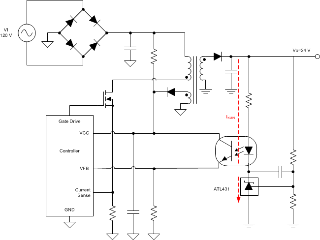 Figure 30. Flyback With Isolation Using ATL43x
 as Voltage Reference and Error Amplifier
10.2 Typical Applications
10.2.1 Comparator with Integrated Reference (Open Loop)
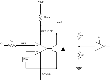 Figure 31. Comparator Application Schematic
10.2.1.1 Design Requirements
For this design example, use the parameters listed in Table 1 as the input parameters.
Table 1. Design Parameters
| DESIGN PARAMETER | EXAMPLE VALUE |
|---|---|
| Input Voltage Range | 0 V to 3.3 V |
| Input Resistance | 100 kΩ |
| Supply Voltage | 5 V |
| Cathode Current (IK) | 50 µA |
| Output Voltage Level | ~2 V - Vsup |
| Logic Input Thresholds VIH/VIL | 1.5 V / 0.8 V |
10.2.1.2 Detailed Design Procedure
When using ATL43x as a comparator with reference, determine the following:
- Input voltage range
- Reference voltage accuracy
- Output logic input high and low level thresholds
- Current source resistance
10.2.1.2.1 Basic Operation
In the configuration shown in Figure 31 ATL43x will behave as a comparator, comparing the Vref pin voltage to the internal virtual reference voltage. When provided a proper cathode current (Ik), ATL43x will have enough open loop gain to provide a quick response. With the ATL43x's max Operating Current (Imin) being 35 µA and up to 40 µA over temperature, operation below that could result in low gain, leading to a slow response.
10.2.1.2.2 Overdrive
Slow or inaccurate responses can also occur when the reference pin is not provided enough overdrive voltage. This is the amount of voltage that is higher than the internal virtual reference. The internal virtual reference voltage will be within the range of 2.5 V ±(0.5% or 1.0%) depending on which version is being used.
The more overdrive voltage provided, the faster the ATL43x will respond.
For applications where ATL43x is being used as a comparator, it is best to set the trip point to greater than the positive expected error (i.e. +1.0% for the A version). For fast response, setting the trip point to > 10% of the internal Vref should suffice. Figure 32 shows the transition from VOH to VOL based on the input voltage and can be used as a guide for selecting the overdrive voltage.
For minimal voltage drop or difference from Vin to the ref pin, it is recommended to use an input resistor < 1 MΩ to provide Iref.
10.2.1.2.3 Output Voltage and Logic Input Level
In order for ATL43x to properly be used as a comparator, the logic output must be readable by the receiving logic device. This is accomplished by knowing the input high and low level threshold voltage levels, typically denoted by VIH & VIL.
As seen in Figure 32, ATL43x's output low level voltage in open-loop/comparator mode is ~2 V, which is sufficient for some ≥ 5.0 V supplied logic. However, would not work for 3.3 V and 1.8 V supplied logic. In order to accommodate this, a resistive divider can be tied to the output to attenuate the output voltage to a voltage legible to the receiving low voltage logic device.
ATL43x's output high voltage is approximately Vsup due to ATL43x being open-collector. If Vsup is much higher than the receiving logic's maximum input voltage tolerance, the output must be attenuated to accommodate the outgoing logic's reliability.
When using a resistive divider on the output, be sure to make the sum of the resistive divider (R1 & R2 in Figure 31) is much greater than Rsup in order to not interfere with ATL43x's ability to pull close to Vsup when turning off.
10.2.1.2.3.1 Input Resistance
ATL43x requires an input resistance in this application in order to source the reference current (Iref) needed from this device to be in the proper operating regions while turning on. The actual voltage seen at the ref pin will be:.
Since Iref can be as high as 0.15 µA it is recommended to use a resistance small enough that will mitigate the error that Iref creates from Vin. Also, the input resistance must be set high enough as to not surpass the absolute maximum of 10mA.
10.2.1.3 Application Curves
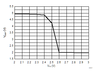
| RIN = 100 kΩ | VSUP = 5.0 V | RSUP = 10 kΩ | |
10.2.2 Shunt Regulator/Reference
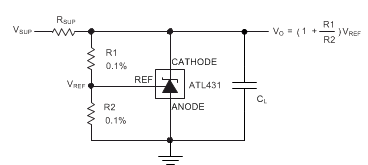 Figure 33. Shunt Regulator Schematic
10.2.2.1 Design Requirements
For this design example, use the parameters listed in Table 2 as the input parameters.
Table 2. Design Parameters
| DESIGN PARAMETER | EXAMPLE VALUE |
|---|---|
| Reference Initial Accuracy | 1.0% |
| Supply Voltage | 48 V |
| Cathode Current (IK) | 50 µA |
| Output Voltage Level | 2.5 V - 36 V |
| Load Capacitance | 1 nF |
| Feedback Resistor Values and Accuracy (R1 & R2) | 10 kΩ |
10.2.2.2 Detailed Design Procedure
When using ATL43x as a Shunt Regulator, determine the following:
- Input voltage range
- Temperature range
- Total accuracy
- Cathode current
- Reference initial accuracy
- Output capacitance
10.2.2.2.1 Programming Output/Cathode Voltage
In order to program the cathode voltage to a regulated voltage a resistive bridge must be shunted between the cathode and anode pins with the mid point tied to the reference pin. This can be seen in Figure 33, with R1 & R2 being the resistive bridge. The cathode/output voltage in the shunt regulator configuration can be approximated by the equation shown in Figure 33. The cathode voltage can be more accuratel determined by taking in to account the cathode current:
In order for this equation to be valid, ATL43x must be fully biased so that it has enough open loop gain to mitigate any gain error. This can be done by meeting the Imin spec denoted in Electrical Characteristics, ATL431Ax, ATL432Ax table.
10.2.2.2.2 Total Accuracy
When programming the output above unity gain (VKA= Vref), ATL43x is susceptible to other errors that may effect the overall accuracy beyond Vref. These errors include:
- R1 and R2 accuracies
- VI(dev) - Change in reference voltage over temperature
- ΔVref / ΔVKA - Change in reference voltage to the change in cathode voltage
- |zKA| - Dynamic impedance, causing a change in cathode voltage with cathode current
Worst case cathode voltage can be determined taking all of the variables in to account. Application note SLVA445 assists designers in setting the shunt voltage to achieve optimum accuracy for this device.
10.2.2.2.3 Stability
Though ATL43x is stable with no capacitive load, the device that receives the shunt regulator's output voltage could present a capacitive load that is within the ATL43x region of stability, shown in Figure 15 through Figure 22. Also, designers may use capacitive loads to improve the transient response or for power supply decoupling.
Figure 15 through Figure 22 should be used as a guide for capacitor selection and compensation. It is characterized using ceramic capacitors with very low ESR. When it is desirable to use a capacitor within the unstable region, higher ESR capacitors can be used to stabilize ATL43x or an external series resistance can be added. For more information and guidance on ESR values, please refer to the application note Designing with the "Advanced" TL431, ATL431SLVA685.
Unlike TL431, the stability boundary is characterized and determined with resistors 250Ω and greater. Which is more suitable for low cathode current applications.
10.2.2.3 Application Curves
