7 Specifications
7.1 Absolute Maximum Ratings(1)
over operating free-air temperature range (unless otherwise noted)
|
|
MIN |
MAX |
UNIT |
| VKA |
Cathode voltage(2) |
|
40 |
V |
| IKA |
Continuous cathode current range |
–100 |
150 |
mA |
| II(ref) |
Reference input current range |
–0.05 |
10 |
mA |
| TJ |
Operating virtual junction temperature |
-40 |
150 |
°C |
| Tstg |
Storage temperature range |
–65 |
150 |
°C |
(1) Stresses beyond those listed under "absolute maximum ratings" may cause permanent damage to the device. These are stress ratings only, and functional operation of the device at these or any other conditions beyond those indicated under "recommended operating conditions" is not implied. Exposure to absolute-maximum-rated conditions for extended periods may affect device reliability.
(2) All voltage values are with respect to ANODE, unless otherwise noted.
7.2 ESD Ratings
|
VALUE |
UNIT |
| V(ESD) |
Electrostatic discharge |
Human-body model (HBM), per ANSI/ESDA/JEDEC JS-001(1) |
±2000 |
V |
| Charged-device model (CDM), per JEDEC specification JESD22-C101(2) |
±1000 |
(1) JEDEC document JEP155 states that 500-V HBM allows safe manufacturing with a standard ESD control process.
(2) JEDEC document JEP157 states that 250-V CDM allows safe manufacturing with a standard ESD control process.
7.3 Thermal Information
| THERMAL METRIC(1) |
ATL43xx |
UNIT |
| DBZ |
| 3 PINS |
| θJA |
Junction-to-ambient thermal resistance |
331.8 |
°C/W |
| θJCtop |
Junction-to-case (top) thermal resistance |
106.5 |
°C/W |
| θJB |
Junction-to-board thermal resistance |
64.6 |
°C/W |
| ψJT |
Junction-to-top characterization parameter |
4.9 |
°C/W |
| ψJB |
Junction-to-board characterization parameter |
62.9 |
°C/W |
(1) For more information about traditional and new thermal metrics, see the IC Package Thermal Metrics application report,
SPRA953.
7.4 Recommended Operating Conditions
|
|
MIN |
MAX |
UNIT |
| VKA |
Cathode voltage |
Vref |
36 |
V |
| IKA |
Cathode current |
.035 |
100 |
mA |
| TA |
Operating free-air temperature |
"I" Grade |
–40 |
85 |
°C |
| "Q" Grade |
–40 |
125 |
7.5 Electrical Characteristics, ATL431Ax, ATL432Ax
over recommended operating conditions, TA = 25°C (unless otherwise noted)
| PARAMETER |
TEST CIRCUIT |
TEST CONDITIONS |
ATL431Ax, ATL432Ax |
UNIT |
| MIN |
TYP |
MAX |
| Vref |
Reference voltage |
Figure 23 |
VKA = Vref, IKA = 1 mA |
2475 |
2500 |
2525 |
mV |
| VI(dev) |
Deviation of reference input voltage over full temperature range, see Notes section |
Figure 23 |
VKA = Vref,
IKA = 1 mA, |
ATL43XAI; TA = -40°C to 85°C |
|
5 |
15 |
mV |
| ATL43XAQ; TA = -40°C to 125°C |
|
6 |
34 |
| ΔVref / ΔVKA |
Ratio of change in reference voltage to the change in cathode voltage |
Figure 24 |
IKA = 1 mA |
ΔVKA = 10 V − Vref |
|
–0.4 |
–2.7 |
mV/V |
| ΔVKA = 36 V − 10 V |
|
–0.1 |
–2 |
| Iref |
Reference input current |
Figure 24 |
IKA = 1 mA, R1 = 10 kΩ, R2 = ∞ |
|
30 |
150 |
nA |
| II(dev) |
Deviation of reference input current over full temperature range, see Notes section |
Figure 24 |
IKA = 1 mA, R1 = 10 kΩ, R2 = ∞ |
|
20 |
50 |
nA |
| Imin |
Minimum cathode current for regulation |
Figure 23
Figure 6 |
VKA = Vref |
|
20 |
35 |
µA |
| Ioff |
Off-state cathode current |
Figure 25 |
VKA = 36 V, Vref = 0 |
|
0.05 |
0.2 |
µA |
| |zKA| |
Dynamic impedance, see Notes section |
Figure 23 |
VKA = Vref, f ≤ 1 kHz, IKA = 1 mA to 100 mA |
|
0.05 |
0.3 |
Ω |
7.6 Electrical Characteristics, ATL431Bx, ATL432Bx
over recommended operating conditions, TA = 25°C (unless otherwise noted)
| PARAMETER |
TEST CIRCUIT |
TEST CONDITIONS |
ATL431Bx, ATL432Bx |
UNIT |
| MIN |
TYP |
MAX |
| Vref |
Reference voltage |
Figure 23 |
VKA = Vref, IKA = 1 mA |
2487 |
2500 |
2512 |
mV |
| VI(dev) |
Deviation of reference input voltage over full temperature range, see Notes section |
Figure 23 |
VKA = Vref, IKA = 1 mA |
ATL43XBI; TA = –40°C to 85°C |
|
5 |
15 |
mV |
| ATL43XBQ; TA = –40°C to 125°C |
|
6 |
34 |
| ΔVref / ΔVKA |
Ratio of change in reference voltage to the change in cathode voltage |
Figure 24 |
IKA = 1 mA |
ΔVKA = 10 V − Vref |
|
–0.4 |
–2.7 |
mV/V |
| ΔVKA = 36 V − 10 V |
|
–0.1 |
–2 |
| Iref |
Reference input current |
Figure 24 |
IKA = 1 mA, R1 = 10 kΩ, R2 = ∞ |
|
30 |
150 |
nA |
| II(dev) |
Deviation of reference input current over full temperature range, see Notes section |
Figure 24 |
IKA = 1 mA, R1 = 10 kΩ, R2 = ∞ |
|
20 |
50 |
nA |
| Imin |
Minimum cathode current for regulation |
Figure 23
Figure 6 |
VKA = Vref |
|
20 |
35 |
µA |
| Ioff |
Off-state cathode current |
Figure 25 |
VKA = 36 V, Vref = 0 |
|
0.05 |
0.2 |
µA |
| |zKA| |
Dynamic impedance, see Notes section |
Figure 23 |
VKA = Vref, f ≤ 1 kHz, IKA = 1 mA to 100 mA |
|
0.05 |
0.3 |
Ω |
7.8 Typical Characteristics
Data at high and low temperatures are applicable only within the recommended operating free-air temperature ranges of the various devices.
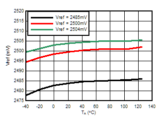
 Figure 2. Reference Voltage vs Free-Air Temperature
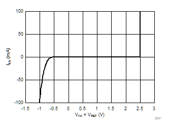
 Figure 4. Cathode Current vs Cathode Voltage
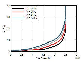
 Figure 6. Cathode Current vs Cathode Voltage
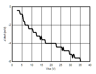
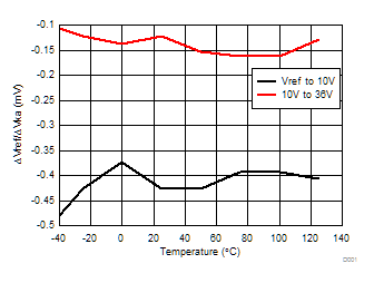
 Figure 8. Delta Reference Voltage vs Cathode Voltage
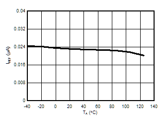
 Figure 3. Reference Current vs Free-Air Temperature
 Figure 5. Cathode Current vs Cathode Voltage
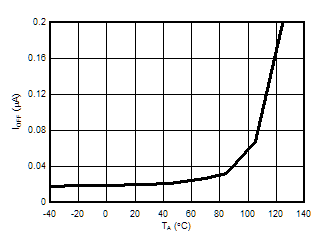
 Figure 7. Off-State Cathode Current vs Free-Air Temperature
 Figure 9. Delta Reference Voltage vs Cathode Voltage
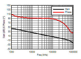
 Figure 11. Small-Signal Voltage Amplification vs Frequency


 which is approximately equal to
