ZHCSJP0A May 2019 – November 2019 ATL431LI-Q1 , ATL432LI-Q1
PRODUCTION DATA.
- 1 特性
- 2 应用
- 3 说明
- 4 修订历史记录
- 5 Device Comparison Table
- 6 Pin Configuration and Functions
- 7 Specifications
- 8 Parameter Measurement Information
- 9 Detailed Description
-
10Applications and Implementation
- 10.1 Application Information
- 10.2
Typical Applications
- 10.2.1 Comparator With Integrated Reference
- 10.2.2 Design Requirements
- 10.2.3 Detailed Design Procedure
- 10.2.4 Application Curves
- 10.2.5 Precision LED Lighting Current Sink Regulator
- 10.2.6 Shunt Regulator/Reference
- 10.2.7 Isolated Flyback with Optocoupler
- 10.2.8 Adjustable Reference for Tracking LDO
- 10.3 System Examples
- 11Power Supply Recommendations
- 12Layout
- 13器件和文档支持
- 14机械、封装和可订购信息
7.6 Typical Characteristics
Data at high and low temperatures are applicable only within the recommended operating free-air temperature ranges of the various devices.
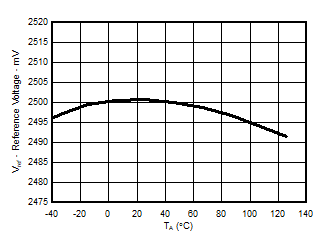 Figure 1. Reference Voltage versus Free-Air Temperature
 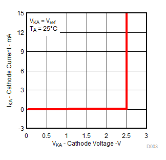 Figure 3. Cathode Current versus Cathode Voltage
 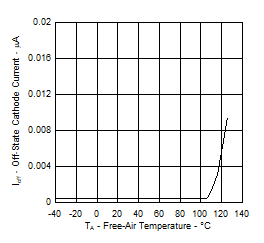 Figure 5. Off-State Cathode Current
versus Free-Air Temperature
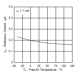 Figure 2. Reference Current versus Free-Air Temperature
 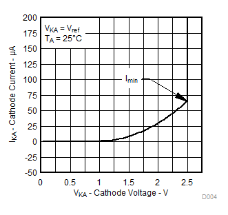 Figure 4. Cathode Current versus Cathode Voltage
 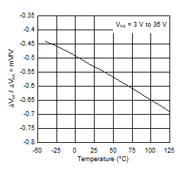 Figure 6. Ratio of Delta Reference Voltage to Delta Cathode Voltage versus Free-Air Temperature
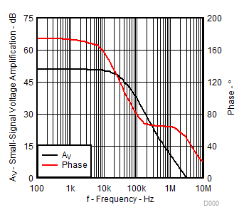
versus Frequency
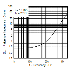 Figure 9. Reference Impedance versus Frequency
 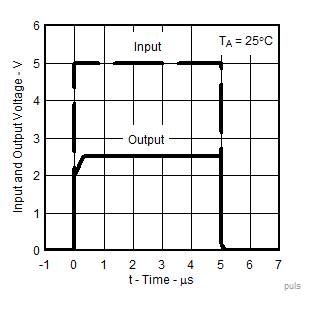 Figure 11. Pulse Response
The areas under the curves represent conditions that may cause the device to oscillate. For curves B and C, R2 and V+ are adjusted to establish the initial VKA and IKA conditions, with CL = 0. VBATT and CL then are adjusted to determine the ranges of stability.
Figure 13. Stability Boundary Conditions for All ATL431LI-Q1, ATL432LI-Q1 Devices Above 1 mA 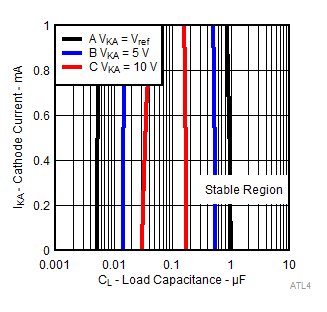
A. The areas in-between the curves represent conditions that may cause the device to oscillate. For curves B and C, R2 and V+ are adjusted to establish the initial VKA and IKA conditions, with CL = 0. VBATT and CL then are adjusted to determine the ranges of stability.
Figure 15. Stability Boundary Conditions for All ATL431LI-Q1, ATL432LI-Q1 Devices Below 1 mA 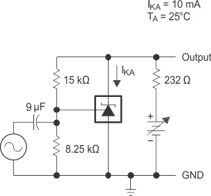 Figure 8. Test Circuit for Voltage Amplification
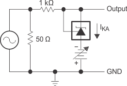
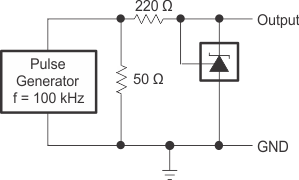
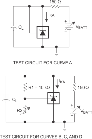 Figure 14. Test Circuit for Stability Boundary Conditions
  Figure 16. Test Circuit for Stability Boundary Conditions