ZHCSHS2C may   2017  – january 2022 AWR1443

PRODUCTION DATA  

  1.   1
  2. 特性
  3. 应用
  4. 说明
  5. 功能方框图
  6. Revision History
  7. Device Comparison
    1. 6.1 Related Products
  8. Terminal Configuration and Functions
    1. 7.1 Pin Diagram
    2. 7.2 Signal Descriptions
      1. 7.2.1 Signal Descriptions
    3. 7.3 Pin Multiplexing
  9. Specifications
    1. 8.1 Absolute Maximum Ratings
    2. 8.2 ESD Ratings
    3. 8.3 Power-On Hours (POH)
    4. 8.4 Recommended Operating Conditions
    5. 8.5 Power Supply Specifications
    6. 8.6 Power Consumption Summary
    7. 8.7 RF Specification
    8. 8.8 Thermal Resistance Characteristics for FCBGA Package [ABL0161]
    9. 8.9 Timing and Switching Characteristics
      1. 8.9.1  Power Supply Sequencing and Reset Timing
      2. 8.9.2  Synchronized Frame Triggering
      3. 8.9.3  Input Clocks and Oscillators
        1. 8.9.3.1 Clock Specifications
      4. 8.9.4  Multibuffered / Standard Serial Peripheral Interface (MibSPI)
        1. 8.9.4.1 Peripheral Description
        2. 8.9.4.2 MibSPI Transmit and Receive RAM Organization
          1. 8.9.4.2.1 SPI Timing Conditions
          2. 8.9.4.2.2 SPI Controller Mode Switching Parameters (CLOCK PHASE = 0, SPICLK = output, SPISIMO = output, and SPISOMI = input) #GUID-C70CFB1F-161A-495B-85B8-62E1C643D037/T4362547-236 #GUID-C70CFB1F-161A-495B-85B8-62E1C643D037/T4362547-237 #GUID-C70CFB1F-161A-495B-85B8-62E1C643D037/T4362547-238
          3. 8.9.4.2.3 SPI Controller Mode Switching Parameters (CLOCK PHASE = 1, SPICLK = output, SPISIMO = output, and SPISOMI = input) #GUID-F724BCC6-8F26-42C4-8723-451EDE9A36D3/T4362547-244 #GUID-F724BCC6-8F26-42C4-8723-451EDE9A36D3/T4362547-245 #GUID-F724BCC6-8F26-42C4-8723-451EDE9A36D3/T4362547-246
        3. 8.9.4.3 SPI Peripheral Mode I/O Timings
          1. 8.9.4.3.1 SPI Peripheral Mode Switching Parameters (SPICLK = input, SPISIMO = input, and SPISOMI = output) #GUID-1B5DE4C6-14B2-48EF-965D-3B03E1AE325B/T4362547-70 #GUID-1B5DE4C6-14B2-48EF-965D-3B03E1AE325B/T4362547-71 #GUID-1B5DE4C6-14B2-48EF-965D-3B03E1AE325B/T4362547-73
        4. 8.9.4.4 Typical Interface Protocol Diagram (Peripheral Mode)
      5. 8.9.5  LVDS Interface Configuration
        1. 8.9.5.1 LVDS Interface Timings
      6. 8.9.6  General-Purpose Input/Output
        1. 8.9.6.1 Switching Characteristics for Output Timing versus Load Capacitance (CL)
      7. 8.9.7  Controller Area Network Interface (DCAN)
        1. 8.9.7.1 Dynamic Characteristics for the DCANx TX and RX Pins
      8. 8.9.8  Serial Communication Interface (SCI)
        1. 8.9.8.1 SCI Timing Requirements
      9. 8.9.9  Inter-Integrated Circuit Interface (I2C)
        1. 8.9.9.1 I2C Timing Requirements #GUID-36963FBF-DA1A-4FF8-B71D-4A185830E708/T4362547-185
      10. 8.9.10 Quad Serial Peripheral Interface (QSPI)
        1. 8.9.10.1 QSPI Timing Conditions
        2. 8.9.10.2 Timing Requirements for QSPI Input (Read) Timings #GUID-6DC69BBB-F187-4499-AC42-8C006552DEE1/T4362547-210 #GUID-6DC69BBB-F187-4499-AC42-8C006552DEE1/T4362547-209
        3. 8.9.10.3 QSPI Switching Characteristics
      11. 8.9.11 JTAG Interface
        1. 8.9.11.1 JTAG Timing Conditions
        2. 8.9.11.2 Timing Requirements for IEEE 1149.1 JTAG
        3. 8.9.11.3 Switching Characteristics Over Recommended Operating Conditions for IEEE 1149.1 JTAG
  10. Detailed Description
    1. 9.1 Overview
    2. 9.2 Functional Block Diagram
    3. 9.3 External Interfaces
    4. 9.4 Subsystems
      1. 9.4.1 RF and Analog Subsystem
        1. 9.4.1.1 Clock Subsystem
        2. 9.4.1.2 Transmit Subsystem
        3. 9.4.1.3 Receive Subsystem
        4. 9.4.1.4 Radio Processor Subsystem
      2. 9.4.2 Main (Control) System
      3. 9.4.3 Host Interface
    5. 9.5 Accelerators and Coprocessors
    6. 9.6 Other Subsystems
      1. 9.6.1 ADC Channels (Service) for User Application
        1. 9.6.1.1 GP-ADC Parameter
    7. 9.7 Boot Modes
      1. 9.7.1 Flashing Mode
      2. 9.7.2 Functional Mode
  11. 10Applications, Implementation, and Layout
    1. 10.1 Application Information
    2. 10.2 Short-Range Radar
    3. 10.3 Blind Spot Detector and Ultrasonic Upgrades
    4. 10.4 Reference Schematic
  12. 11Device and Documentation Support
    1. 11.1 Device Nomenclature
    2. 11.2 Tools and Software
    3. 11.3 Documentation Support
    4. 11.4 支持资源
    5. 11.5 Trademarks
    6. 11.6 静电放电警告
    7. 11.7 术语表
  13. 12Mechanical, Packaging, and Orderable Information
    1. 12.1 Packaging Information

封装选项

请参考 PDF 数据表获取器件具体的封装图。

机械数据 (封装 | 引脚)
  • ABL|161
散热焊盘机械数据 (封装 | 引脚)
订购信息

Flashing Mode

In Flashing Mode, the Main System’s bootloader enables the UART driver and expects a data stream comprising of User Application (Binary Image) and Device Firmware (referred to as Device Firmware Patch or Service Pack) from an external flashing utility. Figure 9-7 shows the flashing utility executing on a PC platform, but the protocol can be accomplished on an embedded platform as well.
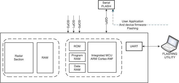
GUID-C33EC45E-5C4A-4B42-96AC-0CF79C662498-low.gifFigure 9-7 Figure 5. Bootloader Flashing Mode