ZHCSL77D April 2020 – January 2022 AWR6443 , AWR6843
PRODUCTION DATA
- 1 特性
- 2 应用
- 3 说明
- 4 功能方框图
- 5 Device Comparison
- 6 Terminal Configuration and Functions
-
7 Specifications
- 7.1 Absolute Maximum Ratings
- 7.2 ESD Ratings
- 7.3 Power-On Hours (POH)
- 7.4 Recommended Operating Conditions
- 7.5 Power Supply Specifications
- 7.6 Power Consumption Summary
- 7.7 RF Specification
- 7.8 CPU Specifications
- 7.9 Thermal Resistance Characteristics for FCBGA Package [ABL0161]
- 7.10
Timing and Switching Characteristics
- 7.10.1 Power Supply Sequencing and Reset Timing
- 7.10.2 Input Clocks and Oscillators
- 7.10.3 Multibuffered / Standard Serial Peripheral Interface (MibSPI)
- 7.10.4 LVDS Interface Configuration
- 7.10.5 General-Purpose Input/Output
- 7.10.6 Controller Area Network - Flexible Data-rate (CAN-FD)
- 7.10.7 Serial Communication Interface (SCI)
- 7.10.8 Inter-Integrated Circuit Interface (I2C)
- 7.10.9 Quad Serial Peripheral Interface (QSPI)
- 7.10.10 ETM Trace Interface
- 7.10.11 Data Modification Module (DMM)
- 7.10.12 JTAG Interface
- 8 Detailed Description
- 9 Monitoring and Diagnostics
- 10Applications, Implementation, and Layout
- 11Device and Documentation Support
- 12Mechanical, Packaging, and Orderable Information
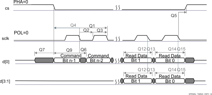
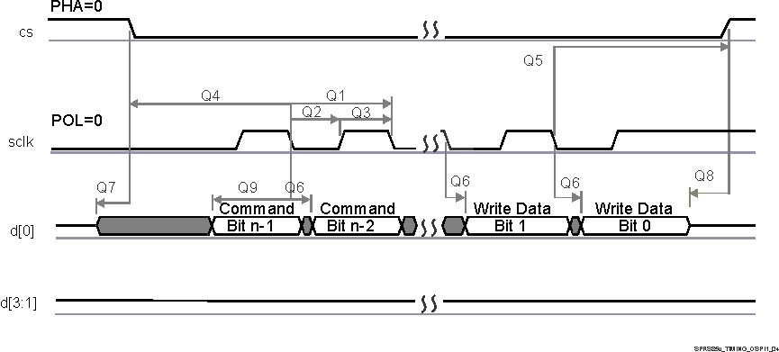
7.10.9.3 QSPI Switching Characteristics
| NO. | PARAMETER | MIN | TYP | MAX | UNIT | |
|---|---|---|---|---|---|---|
| Q1 | tc(SCLK) | Cycle time, sclk | 12.5 | ns | ||
| Q2 | tw(SCLKL) | Pulse duration, sclk low | Y*P – 3(1)(2) | ns | ||
| Q3 | tw(SCLKH) | Pulse duration, sclk high | Y*P – 3(1) | ns | ||
| Q4 | td(CS-SCLK) | Delay time, sclk falling edge to cs active edge | –M*P – 1(1)(3) | –M*P + 2.5(1)(3) | ns | |
| Q5 | td(SCLK-CS) | Delay time, sclk falling edge to cs inactive edge | N*P – 1(1)(3) | N*P + 2.5(1)(3) | ns | |
| Q6 | td(SCLK-D1) | Delay time, sclk falling edge to d[1] transition | –2.5 | 4 | ns | |
| Q7 | tena(CS-D1LZ) | Enable time, cs active edge to d[1] driven (lo-z) | –P – 4(3) | –P +1(3) | ns | |
| Q8 | tdis(CS-D1Z) | Disable time, cs active edge to d[1] tri-stated (hi-z) | –P – 4(3) | –P +1(3) | ns | |
| Q9 | td(SCLK-D1) | Delay time, sclk first falling edge to first d[1] transition (for PHA = 0 only) | –2.5 – P(3) | 4 – P(3) | ns | |
| Q12 | tsu(D-SCLK) | Setup time, d[3:0] valid before falling sclk edge | 5 | ns | ||
| Q13 | th(SCLK-D) | Hold time, d[3:0] valid after falling sclk edge | 1 | ns | ||
| Q14 | tsu(D-SCLK) | Setup time, final d[3:0] bit valid before final falling sclk edge | 5 — P(3) | ns | ||
| Q15 | th(SCLK-D) | Hold time, final d[3:0] bit valid after final falling sclk edge | 1 + P(3) | ns | ||
(1) The Y parameter is defined as follows: If DCLK_DIV is 0 or ODD then, Y equals 0.5. If DCLK_DIV is EVEN then, Y equals (DCLK_DIV/2) / (DCLK_DIV+1). For best performance, it is recommended to use a DCLK_DIV of 0 or ODD to minimize the duty cycle distortion. All required details about clock division factor DCLK_DIV can be found in the device-specific Technical Reference Manual.
(2) P = SCLK period in ns.
(3) M = QSPI_SPI_DC_REG.DDx + 1, N = 2
 Figure 7-14 QSPI Read (Clock Mode 0)
 Figure 7-15 QSPI Write (Clock Mode 0)