ZHCSGY5A October   2017  – December 2017

PRODUCTION DATA.  

  1. 特性
  2. 应用范围
  3. 说明
    1.     典型应用电路
  4. 修订历史记录
  5. 说明 (续)
  6. Device Comparison Table
  7. Pin Configuration and Functions
    1.     Pin Functions
    2. 7.1 EN1/EN2 Settings
  8. Specifications
    1. 8.1 Absolute Maximum Ratings
    2. 8.2 ESD Ratings
    3. 8.3 Recommended Operating Conditions
    4. 8.4 Thermal Information
    5. 8.5 Dissipation Ratings
    6. 8.6 Electrical Characteristics
    7. 8.7 Typical Characteristics
  9. Detailed Description
    1. 9.1 Overview
    2. 9.2 Functional Block Diagram
    3. 9.3 Feature Description
      1. 9.3.1 Undervoltage Lockout (UVLO)
      2. 9.3.2 Power On
      3. 9.3.3 Overvoltage Protection (OVP)
      4. 9.3.4 Dynamic Power-Path Management
        1. 9.3.4.1 Input Source Connected (ADAPTER or USB)
          1. 9.3.4.1.1 Input DPM Mode (VIN-DPM)
          2. 9.3.4.1.2 DPPM Mode
          3. 9.3.4.1.3 Battery Supplement Mode
        2. 9.3.4.2 Input Source Not Connected
      5. 9.3.5 Battery Charging
        1. 9.3.5.1 Charge Current Translator
        2. 9.3.5.2 Battery Detection and Recharge
        3. 9.3.5.3 Battery Disconnect (SYSOFF Input, bq24076, bq24078)
        4. 9.3.5.4 Dynamic Charge Timers (TMR Input)
        5. 9.3.5.5 Status Indicators (PGOOD, CHG)
        6. 9.3.5.6 Thermal Regulation and Thermal Shutdown
      6. 9.3.6 Battery Pack Temperature Monitoring
    4. 9.4 Device Functional Modes
      1. 9.4.1 Sleep Mode
      2. 9.4.2 Explanation of Deglitch Times and Comparator Hysteresis
  10. 10Application and Implementation
    1. 10.1 Application Information
    2. 10.2 Typical Application
      1. 10.2.1 Design Requirements
      2. 10.2.2 Detailed Design Procedure
        1. 10.2.2.1 bq2407x Charger Design Example
          1. 10.2.2.1.1 System ON/OFF (SYSOFF) (bq24076 or bq24078 only)
        2. 10.2.2.2 Calculations
          1. 10.2.2.2.1 Program the Fast Charge Current (ISET):
          2. 10.2.2.2.2 Program the Input Current Limit (ILIM)
          3. 10.2.2.2.3 Program 6.25-hour Fast-Charge Safety Timer (TMR)
        3. 10.2.2.3 TS Function
        4. 10.2.2.4 CHG and PGOOD
        5. 10.2.2.5 Selecting IN, OUT, and BAT Pin Capacitors
      3. 10.2.3 Application Curves
  11. 11Power Supply Recommendations
  12. 12Layout
    1. 12.1 Layout Guidelines
    2. 12.2 Layout Example
    3. 12.3 Thermal Considerations
  13. 13器件和文档支持
    1. 13.1 器件支持
      1. 13.1.1 Third-Party Products Disclaimer
    2. 13.2 相关链接
    3. 13.3 接收文档更新通知
    4. 13.4 社区资源
    5. 13.5 商标
    6. 13.6 静电放电警告
    7. 13.7 Glossary
  14. 14机械、封装和可订购信息

封装选项

机械数据 (封装 | 引脚)
散热焊盘机械数据 (封装 | 引脚)
订购信息

Thermal Regulation and Thermal Shutdown

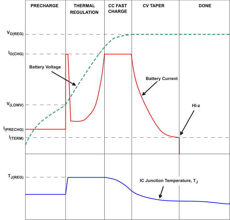
The bq2407x contain a thermal regulation loop that monitors the die temperature. If the temperature exceeds TJ(REG), the device automatically reduces the charging current to prevent the die temperature from increasing further. In some cases, the die temperature continues to rise despite the operation of the thermal loop, particularly under high VIN and heavy OUT system load conditions. Under these conditions, if the die temperature increases to TJ(OFF), the input FET Q1 is turned OFF. FET Q2 is turned ON to ensure that the battery still powers the load on OUT. Once the device die temperature cools by TJ(OFF-HYS), the input FET Q1 is turned on and the device returns to thermal regulation. Continuous overtemperature conditions result in a "hiccup" mode. During thermal regulation, the safety timers are slowed down proportionately to the reduction in current limit.

Note that this feature monitors the die temperature of the bq2407x. This is not synonymous with ambient temperature. Self heating exists due to the power dissipated in the IC because of the linear nature of the battery charging algorithm and the LDO associated with OUT. A modified charge cycle with the thermal loop active is shown in Figure 19. Battery termination is disabled during thermal regulation.
bq24076 bq24078 mod_chg_cyc_lus810.gifFigure 19. Charge Cycle Modified by Thermal Loop