ZHCSLN5D december 2010 – september 2020 BQ24133
PRODUCTION DATA
- 1
- 1 特性
- 2 应用
- 3 说明
- 4 Revision History
- 5 Description (continued)
- 6 Device Comparison Table
- 7 Pin Configuration and Functions
- 8 Specifications
-
9 Detailed Description
- 9.1 Overview
- 9.2 Functional Block Diagram
- 9.3
Feature Description
- 9.3.1 Battery Voltage Regulation
- 9.3.2 Battery Current Regulation
- 9.3.3 Battery Precharge Current Regulation
- 9.3.4 Input Current Regulation
- 9.3.5 Charge Termination, Recharge, And Safety Timers
- 9.3.6 Power Up
- 9.3.7 Input Undervoltage Lockout (UVLO)
- 9.3.8 Input Overvoltage/Undervoltage Protection
- 9.3.9 Enable and Disable Charging
- 9.3.10 System Power Selector
- 9.3.11 Converter Operation
- 9.3.12 Automatic Internal Soft-Start Charger Current
- 9.3.13 Charge Overcurrent Protection
- 9.3.14 Charge Undercurrent Protection
- 9.3.15 Battery Detection
- 9.3.16 Battery Short Protection
- 9.3.17 Battery Overvoltage Protection
- 9.3.18 Temperature Qualification
- 9.3.19 MOSFET Short Circuit and Inductor Short Circuit Protection
- 9.3.20 Thermal Regulation and Shutdown Protection
- 9.3.21 Timer Fault Recovery
- 9.3.22 Charge Status Outputs
- 9.4 Device Functional Modes
- 10Application and Implementation
- 11Power Supply Recommendations
- 12Layout
- 13Device and Documentation Support
- 14Mechanical, Packaging, and Orderable Information
10.2.2.5 Input ACFET and RBFET Selection
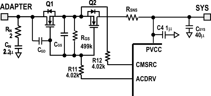
N-type MOSFETs are used as input ACFET(Q1) and RBFET(Q2) for better cost-effective and small-size solution, as shown in Figure 22. Normally, there is a total capacitance of 50 µH connected at PVCC node: 10-µF capacitor for buck converter of BQ24133 and 40-µF capacitor for system side. There is a surge current during Q1 turnon period when a valid adapter is inserted. Decreasing the turnon speed of Q1 can limit this surge current in desirable range by selecting a MOSFET with relative bigger CGD and/or CGS. If Q1 turns on too fast, we must add external CGD and/or CGS. For example, 4.7-nF CGD and 47-nF CGS are adopted on EVM while using NexFET CSD17313 as Q1.
 Figure 10-3 Input ACFET and RBFET