ZHCS384H November 2011 – July 2022 BQ24160 , BQ24160A , BQ24161 , BQ24161B , BQ24163 , BQ24168
PRODUCTION DATA
- 1 特性
- 2 应用
- 3 说明
- 4 Revision History
- 5 Device Comparison Table
- 6 Pin Configuration and Functions
- 7 Specifications
-
8 Detailed Description
- 8.1 Overview
- 8.2 Functional Block Diagram
- 8.3
Feature Description
- 8.3.1 Charge Mode Operation
- 8.3.2 Battery Charging Process
- 8.3.3 Battery Detection
- 8.3.4 Dynamic Power Path Management (DPPM)
- 8.3.5 Input Source Connected
- 8.3.6 Battery Only Connected
- 8.3.7 Battery Discharge FET (BGATE)
- 8.3.8 DEFAULT Mode
- 8.3.9 Safety Timer and Watchdog Timer (BQ24160/BQ24161/BQ24161B/BQ24163 only)
- 8.3.10 D+, D– Based Adapter Detection for the USB Input (D+, D–, BQ24160/0A/3)
- 8.3.11 USB Input Current Limit Selector Input (PSEL, BQ24161/161B/168 only)
- 8.3.12 Hardware Chip Disable Input (CD)
- 8.3.13 LDO Output (DRV)
- 8.3.14 External NTC Monitoring (TS)
- 8.3.15 Thermal Regulation and Protection
- 8.3.16 Input Voltage Protection in Charge Mode
- 8.3.17 Charge Status Outputs (STAT, INT)
- 8.3.18 Good Battery Monitor
- 8.4 Device Functional Modes
- 8.5 Programming
- 8.6
Register Maps
- 8.6.1 Status/Control Register (READ/WRITE)
- 8.6.2 Battery/ Supply Status Register (READ/WRITE)
- 8.6.3 Control Register (READ/WRITE)
- 8.6.4 Control/Battery Voltage Register (READ/WRITE)
- 8.6.5 Vender/Part/Revision Register (READ only)
- 8.6.6 Battery Termination/Fast Charge Current Register (READ/WRITE)
- 8.6.7 VIN-DPM Voltage/ DPPM Status Register
- 8.6.8 Safety Timer/ NTC Monitor Register (READ/WRITE)
- 9 Application and Implementation
- 10Power Supply Recommendations
- 11Layout
- 12Device and Documentation Support
封装选项
机械数据 (封装 | 引脚)
散热焊盘机械数据 (封装 | 引脚)
- RGE|24
订购信息
8.5.1.1 F/S Mode Protocol
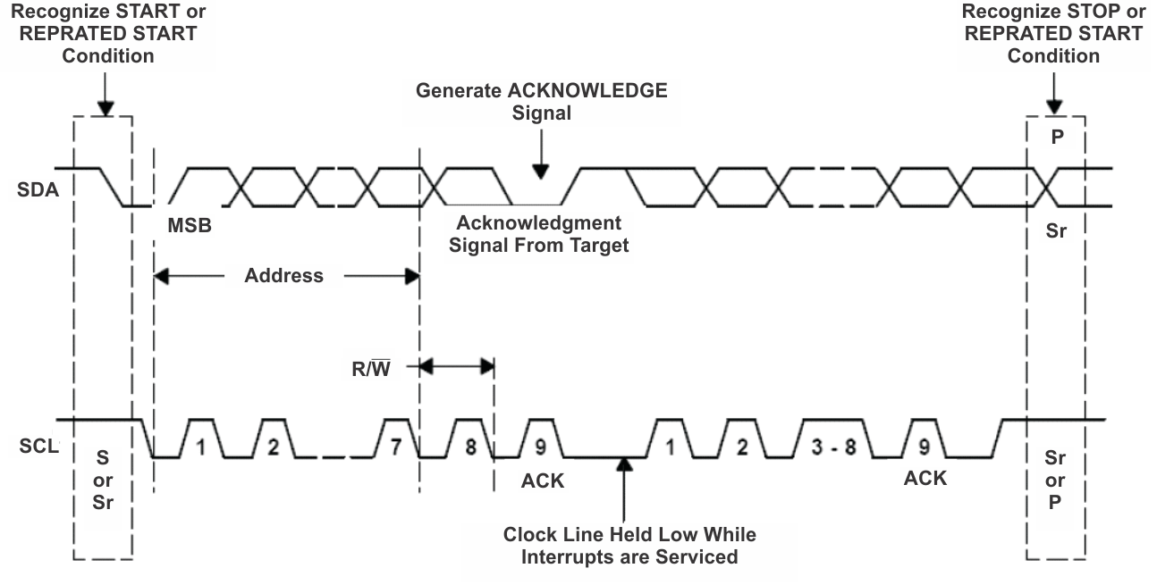
The host initiates data transfer by generating a start condition. The start condition is when a high-to-low transition occurs on the SDA line while SCL is high, as shown in Figure 8-8. All I2C-compatible devices should recognize a start condition.
 Figure 8-8 START and STOP Condition
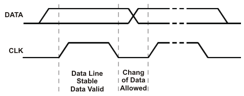
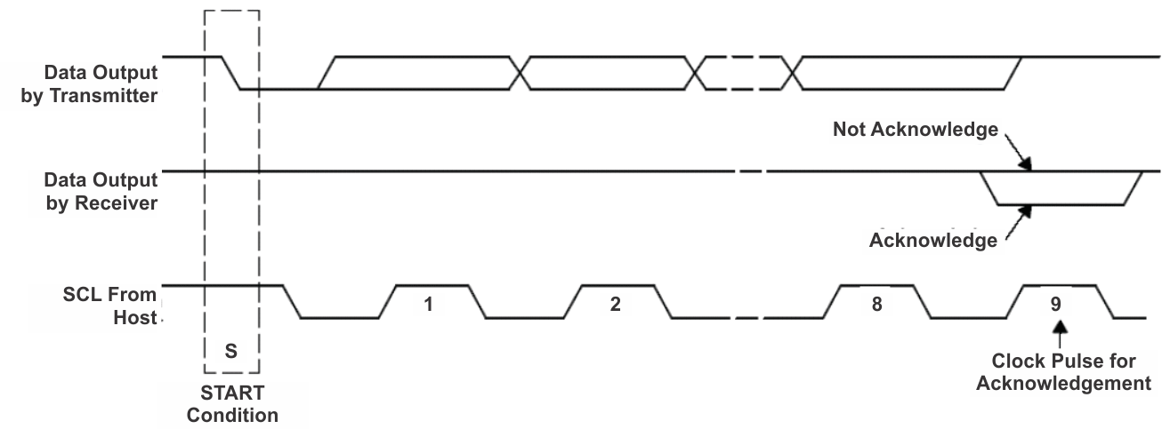
The host then generates the SCL pulses, and transmits the 8-bit address and the read/write direction bit R/W on the SDA line. During all transmissions, the host ensures that data is valid. A valid data condition requires the SDA line to be stable during the entire high period of the clock pulse (see Figure 8-9). All devices recognize the address sent by the host and compare it to their internal fixed addresses. Only the target device with a matching address generates an acknowledge (see Figure 8-10) by pulling the SDA line low during the entire high period of the ninth SCL cycle. Upon detecting this acknowledge, the host knows that communication link with a target has been established.
 Figure 8-9 Bit Transfer on the Serial Interface
The host generates further SCL cycles to either transmit data to the target (R/W bit 1) or receive data from the target (R/W bit 0). In either case, the receiver needs to acknowledge the data sent by the transmitter. So an acknowledge signal can either be generated by the host or by the target, depending on which one is the receiver. The 9-bit valid data sequences consisting of 8-bit data and 1-bit acknowledge can continue as long as necessary. To signal the end of the data transfer, the host generates a stop condition by pulling the SDA line from low to high while the SCL line is high (see Figure 8-11). This releases the bus and stops the communication link with the addressed target. All I2C compatible devices must recognize the stop condition. Upon the receipt of a stop condition, all devices know that the bus is released, and wait for a start condition followed by a matching address. If a transaction is terminated prematurely, the host needs sending a STOP condition to prevent the target I2C logic from remaining in an incorrect state. Attempting to read data from register addresses not listed in this section result in FFh being read out.
 Figure 8-10 Acknowledge on the
I2C Bus
 Figure 8-11 Bus Protocol