ZHCSAD3B January   2012  – December 2014

PRODUCTION DATA.  

  1. 特性
  2. 应用
  3. 说明
  4. 修订历史记录
  5. 说明 (续)
  6. Device Comparison Table
  7. Pin Configuration and Functions
  8. Specifications
    1. 8.1 Absolute Maximum Ratings
    2. 8.2 ESD Ratings
    3. 8.3 Recommended Operating Conditions
    4. 8.4 Thermal Information
    5. 8.5 Electrical Characteristics
    6. 8.6 Typical Characteristics
  9. Detailed Description
    1. 9.1 Overview
    2. 9.2 Functional Block Diagram
    3. 9.3 Feature Description
      1. 9.3.1 Device Power Up
        1. 9.3.1.1 Power-On-Reset (POR)
        2. 9.3.1.2 Power Up from Battery without DC Source
          1. 9.3.1.2.1 BATFET Turn Off
          2. 9.3.1.2.2 Shipping Mode
        3. 9.3.1.3 Power Up from DC Source
          1. 9.3.1.3.1 REGN LDO
          2. 9.3.1.3.2 Input Source Qualification
          3. 9.3.1.3.3 Input Current Limit Detection
          4. 9.3.1.3.4 D+/D- Detection Sets Input Current Limit in bq24190
          5. 9.3.1.3.5 PSEL/OTG Pins Set Input Current Limit in bq24192, bq24192I
          6. 9.3.1.3.6 HIZ State wth 100mA USB Host
          7. 9.3.1.3.7 Force Input Current Limit Detection
        4. 9.3.1.4 Converter Power-Up
        5. 9.3.1.5 Boost Mode Operation from Battery
      2. 9.3.2 Power Path Management
        1. 9.3.2.1 Narrow VDC Architecture
        2. 9.3.2.2 Dynamic Power Management
        3. 9.3.2.3 Supplement Mode
      3. 9.3.3 Battery Charging Management
        1. 9.3.3.1 Autonomous Charging Cycle
        2. 9.3.3.2 Battery Charging Profile
        3. 9.3.3.3 Battery Path Impedance IR Compensation
        4. 9.3.3.4 Thermistor Qualification
          1. 9.3.3.4.1 Cold/Hot Temperature Window
        5. 9.3.3.5 Charging Termination
          1. 9.3.3.5.1 Termination when REG02[0] = 1
          2. 9.3.3.5.2 Termination when REG05[6] = 1
        6. 9.3.3.6 Charging Safety Timer
        7. 9.3.3.7 USB Timer when Charging from USB100mA Source
      4. 9.3.4 Status Outputs (PG, STAT, and INT)
        1. 9.3.4.1 Power Good Indicator (PG)
        2. 9.3.4.2 Charging Status Indicator (STAT)
        3. 9.3.4.3 Interrupt to Host (INT)
      5. 9.3.5 Protections
        1. 9.3.5.1 Input Current Limit on ILIM
        2. 9.3.5.2 Thermal Regulation and Thermal Shutdown
        3. 9.3.5.3 Voltage and Current Monitoring in Buck Mode
          1. 9.3.5.3.1 Input Over-Voltage (ACOV)
          2. 9.3.5.3.2 System Over-Voltage Protection (SYSOVP)
        4. 9.3.5.4 Voltage and Current Monitoring in Boost Mode
          1. 9.3.5.4.1 VBUS Over-Voltage Protection
        5. 9.3.5.5 Battery Protection
          1. 9.3.5.5.1 Battery Over-Current Protection (BATOVP)
          2. 9.3.5.5.2 Charging During Battery Short Protection
          3. 9.3.5.5.3 System Over-Current Protection
      6. 9.3.6 Serial Interface
        1. 9.3.6.1 Data Validity
        2. 9.3.6.2 START and STOP Conditions
        3. 9.3.6.3 Byte Format
        4. 9.3.6.4 Acknowledge (ACK) and Not Acknowledge (NACK)
        5. 9.3.6.5 Slave Address and Data Direction Bit
          1. 9.3.6.5.1 Single Read and Write
          2. 9.3.6.5.2 Multi-Read and Multi-Write
    4. 9.4 Device Functional Modes
      1. 9.4.1 Host Mode and Default Mode
        1. 9.4.1.1 Plug in USB100mA Source with Good Battery
        2. 9.4.1.2 USB Timer when Charging from USB 100-mA Source
    5. 9.5 Register Map
      1. 9.5.1 I2C Registers
        1. 9.5.1.1  Input Source Control Register REG00 (bq24190, bq24192 reset = 00110000, or 30; bq24192I reset = 00111000, or 38)
        2. 9.5.1.2  Power-On Configuration Register REG01 (reset = 00011011, or 1B)
        3. 9.5.1.3  Charge Current Control Register REG02 (bq24190, bq24192 reset = 01100000, or 60; bq24192I reset = 00100000, or 20)
        4. 9.5.1.4  Pre-Charge/Termination Current Control Register REG03 (reset = 00010001, or 11)
        5. 9.5.1.5  Charge Voltage Control Register REG04 (bq24190, bq241192 reset = 10110010, or B2; bq24192I reset = 10011010, or 9A)
        6. 9.5.1.6  Charge Termination/Timer Control Register REG05 (reset = 10011010, or 9A)
        7. 9.5.1.7  IR Compensation / Thermal Regulation Control Register REG06 (reset = 00000011, or 03)
        8. 9.5.1.8  Misc Operation Control Register REG07 (reset = 01001011, or 4B)
        9. 9.5.1.9  System Status Register REG08
        10. 9.5.1.10 Fault Register REG09
        11. 9.5.1.11 Vender / Part / Revision Status Register REG0A (bq24190 reset = 00100011, or 23; bq24192 reset = 00101011, or 2B; bq24192I reset = 00001011, or 0B)
  10. 10Application and Implementation
    1. 10.1 Application Information
    2. 10.2 Typical Application
      1. 10.2.1 Design Requirements
      2. 10.2.2 Detailed Design Procedure
        1. 10.2.2.1 Inductor Selection
        2. 10.2.2.2 Input Capacitor
        3. 10.2.2.3 Output Capacitor
      3. 10.2.3 Application Performance Plots
  11. 11Power Supply Recommendations
  12. 12Layout
    1. 12.1 Layout Guidelines
    2. 12.2 Layout Example
  13. 13器件和文档支持
    1. 13.1 文档支持
      1. 13.1.1 相关文档
    2. 13.2 相关链接
    3. 13.3 商标
    4. 13.4 静电放电警告
    5. 13.5 术语表
  14. 14机械、封装和可订购信息

封装选项

机械数据 (封装 | 引脚)
散热焊盘机械数据 (封装 | 引脚)
订购信息

8 Specifications

8.1 Absolute Maximum Ratings(1)

over operating free-air temperature range (unless otherwise noted)
MIN MAX UNIT
Voltage range (with respect to GND) VBUS –2 22 V
PMID –0.3 22 V
STAT, PG –0.3 20 V
BTST –0.3 26 V
SW –2 20 V
BAT, SYS (converter not switching) –0.3 6 V
SDA, SCL, INT, OTG, ILIM, REGN, TS1, TS2, CE, PSEL, D+, D– –0.3 7 V
BTST TO SW –0.3 –7 V
PGND to GND –0.3 –0.3 V
Output sink current INT, STAT, PG 6 mA
Junction temperature –40°C 150 °C
Storage temperature, Tstg –65 150 °C
(1) Stresses beyond those listed under absolute maximum ratings may cause permanent damage to the device. These are stress ratings only, and functional operation of the device at these or any other conditions beyond those indicated under recommended operating conditions is not implied. Exposure to absolute-maximum-rated conditions for extended periods may affect device reliability. All voltage values are with respect to the network ground terminal unless otherwise noted.

8.2 ESD Ratings

VALUE UNIT
V(ESD) Electrostatic discharge Human body model (HBM), per ANSI/ESDA/JEDEC JS-001(1) 1000 V
Charged device model (CDM), per JEDEC specification JESD22-C101(2) 250
(1) JEDEC document JEP155 states that 500-V HBM allows safe manufacturing with a standard ESD control process.
(2) JEDEC document JEP157 states that 250-V CDM allows safe manufacturing with a standard ESD control process.

8.3 Recommended Operating Conditions

MIN MAX UNIT
VIN Input voltage 3.9 17(1) V
IIN Input current 3 A
ISYS Output current (SYS) 4.5 A
VBAT Battery voltage 4.4 V
IBAT Fast charging current 4.5 A
Discharging current with internal MOSFET 6 (continuous)
9 (peak)
(up to 1 sec duration)
A
TA Operating free-air temperature range –40 85 °C
(1) The inherent switching noise voltage spikes should not exceed the absolute maximum rating on either the BTST or SW pins. A tight layout minimizes switching noise.

8.4 Thermal Information

THERMAL METRIC(1) bq2419x UNIT
RGE (24 PIN)
RθJA Junction-to-ambient thermal resistance 32.2 °C/W
RθJCtop Junction-to-case (top) thermal resistance 29.8
RθJB Junction-to-board thermal resistance 9.1
ψJT Junction-to-top characterization parameter 0.3
ψJB Junction-to-board characterization parameter 9.1
RθJCbot Junction-to-case (bottom) thermal resistance 2.2
(1) For more information about traditional and new thermal metrics, see the IC Package Thermal Metrics application report, SPRA953.

8.5 Electrical Characteristics

VVBUS_UVLOZ < VVBUS < VACOV and VVBUS > VBAT + VSLEEP, TJ = –40°C to 125°C and TJ = 25°C for typical values unless other noted.
PARAMETER TEST CONDITIONS MIN TYP MAX UNIT
QUIESCENT CURRENTS
IBAT Battery discharge current (BAT, SW, SYS) VVBUS < VUVLO, VBAT = 4.2 V, leakage between BAT and VBUS 5 µA
High-Z Mode, or no VBUS, BATFET disabled (REG07[5] = 1), –40°C to 85°C 12 20 µA
High-Z Mode, or no VBUS, REG07[5] = 0, –40°C to 85°C 32 55 µA
IVBUS Input supply current (VBUS) VVBUS = 5 V, High-Z mode 15 30 µA
VVBUS = 17 V, High-Z mode 30 50 µA
VVBUS > VUVLO, VVBUS > VBAT, converter not switching 1.5 3 mA
VVBUS > VUVLO, VVBUS > VBAT, converter switching, VBAT = 3.2 V, ISYS = 0 A 4 mA
VVBUS > VUVLO, VVBUS > VBAT, converter switching, VBAT = 3.8 V, ISYS = 0 A 15 mA
IOTGBOOST Battery discharge current in boost mode VBAT = 4.2 V, Boost mode, IVBUS = 0 A, converter switching 4 mA
VBUS/BAT POWER UP
VVBUS_OP VBUS operating range 3.9 17 V
VVBUS_UVLOZ VBUS for active I2C, no battery VVBUS rising 3.6 V
VSLEEP Sleep mode falling threshold VVBUS falling, VVBUS-VBAT 35 80 120 mV
VSLEEPZ Sleep mode rising threshold VVBUS rising, VVBUS-VBAT 170 250 350 mV
VACOV VBUS over-voltage rising threshold VVBUS rising 17.4 18 V
VACOV_HYST VBUS over-voltage falling hysteresis VVBUS falling 700 mV
VBAT_UVLOZ Battery for active I2C, no VBUS VBAT rising 2.3 V
VBAT_DPL Battery depletion threshold VBAT falling 2.4 2.6 V
VBAT_DPL_HY Battery depletion rising hysteresis VBAT rising 170 260 mV
VVBUSMIN Bad adapter detection threshold VVBUS falling 3.8 V
IBADSRC Bad adapter detection current source 30 mA
tBADSRC Bad source detection duration 30 ms
POWER PATH MANAGEMENT
VSYS_RANGE Typical system regulation voltage Isys = 0 A, Q4 off, VBAT up to 4.2 V,
REG01[3:1] = 101, VSYSMIN = 3.5 V
3.5 4.35 V
VSYS_MIN System voltage output REG01[3:1] = 101, VSYSMIN = 3.5 V 3.55 3.65 V
RON(RBFET) Internal top reverse blocking MOSFET on-resistance Measured between VBUS and PMID 23 38
RON(HSFET) Internal top switching MOSFET on-resistance between PMID and SW TJ = –40°C to 85°C 27 35
TJ = -40°C to 125°C 27 45
RON(LSFET) Internal bottom switching MOSFET on-resistance between SW and PGND TJ = –40°C to 85°C 32 45
TJ = -40°C to 125°C 32 48
VFWD BATFET forward voltage in supplement mode BAT discharge current 10 mA 30 mV
VSYS_BAT SYS/BAT Comparator VSYS falling 90 mV
VBATGD Battery good comparator rising threshold VBAT rising 3.55 V
VBATGD_HYST Battery good comparator falling threshold VBAT falling 100 mV
BATTERY CHARGER
VBAT_REG_ACC Charge voltage regulation accuracy VBAT = 4.112 V and 4.208 V –0.5% 0.5%
IICHG_REG_ACC Fast charge current regulation accuracy VBAT = 3.8 V, ICHG = 1792 mA, TJ = 25°C –4% 4%
VBAT = 3.8 V, ICHG = 1792 mA, TJ = –20°C to 125°C –7% 7%
ICHG_20pct Charge current with 20% option on VBAT = 3.1 V, ICHG = 104 mA, REG02 = 03 75 100 150 mA
VBATLOWV Battery LOWV falling threshold Fast charge to precharge, REG04[1] = 1 2.6 2.8 2.9 V
VBATLOWV_HYST Battery LOWV rising threshold Precharge to fast charge, REG04[1] = 1 2.8 3.0 3.1 V
IPRECHG_ACC Precharge current regulation accuracy VBAT = 2.6 V, ICHG = 256 mA –20% 20%
ITERM_ACC Termination current accuracy ITERM = 256 mA, ICHG = 960 mA –20% 20%
VSHORT Battery Short Voltage VBAT falling 2.0 V
VSHORT_HYST Battery Short Voltage hysteresis VBAT rising 200 mV
ISHORT Battery short current VBAT < 2.2V 100 mA
VRECHG Recharge threshold below VBAT_REG VBAT falling, REG04[0] = 0 100 mV
tRECHG Recharge deglitch time VBAT falling, REG04[0] = 0 20 ms
RON_BATFET SYS-BAT MOSFET on-resistance TJ = 25°C 12 15
TJ = –40°C to 125°C 12 20
INPUT VOLTAGE/CURRENT REGULATION
VINDPM_REG_ACC Input voltage regulation accuracy REG00[6:3] = 0110 (4.36 V) or 1011 (4.76 V) –2% 2%
IUSB_DPM USB Input current regulation limit, VBUS = 5 V, current pulled from SW USB100 85 100 mA
USB150 125 150 mA
USB500 440 500 mA
USB900 750 900 mA
IADPT_DPM Input current regulation accuracy Typical input current of 1.5 A based on KLIM 1.35 1.5 1.65 A
IIN_START Input current limit during system start up VSYS < 2.2 V 100 mA
KILIM IIN = KILIM/RILIM IINDPM = 1.5 A 435 485 530 A x Ω
D+/D- DETECTION
VD+_SRC D+ voltage source 0.5 0.6 0.7 V
ID+_SRC D+ connection check current source 7 14 µA
ID–_SINK D– current sink 50 100 150 µA
ID_LKG Leakage current into D+/D– D–, switch open –1 1 µA
D+, switch open –1 1 µA
VD+_LOW D+ Low comparator threshold 0.7 0.8 V
VD–_LOWdatref D– Low comparator threshold 250 400 mV
RD–_DWN D– Pulldown for connection check 14.25 24.8
tSDP_DEFAULT Charging timer with 100-mA USB host in default mode 45 mins
BAT OVER-VOLTAGE PROTECTION
VBATOVP Battery over-voltage threshold VBAT rising, as percentage of VBAT_REG 104%
VBATOVP_HYST Battery over-voltage hysteresis VBAT falling, as percentage of VBAT_REG 2%
tBATOVP Battery over-voltage deglitch time to disable charge 1 µs
THERMAL REGULATION AND THERMAL SHUTDOWN
TJunction_REG Junction temperature regulation accuracy REG06[1:0] = 11 120 °C
TSHUT Thermal shutdown rising temperature Temperature increasing 160 °C
TSHUT_HYS Thermal shutdown hysteresis 30 °C
Thermal shutdown rising deglitch Temperature increasing delay 1 ms
Thermal shutdown falling deglitch Temperature decreasing delay 1 ms
COLD/HOT THERMISTER COMPARATOR (bq24190,bq24192,bq24192I)
VLTF Cold temperature threshold, TS pin voltage rising threshold Charger suspends charge. As percentage to VREGN 73% 73.5% 74%
VLTF_HYS Cold temperature hysteresis, TS pin voltage falling As percentage to VREGN 0.2% 0.4% 0.6%
VHTF Hot temperature TS pin voltage rising threshold As percentage to VREGN 46.6% 47.2% 48.8%
VTCO Cut-off temperature TS pin voltage falling threshold As percentage to VREGN 44.2% 44.7% 45.2%
Deglitch time for temperature out of range detection VTS > VLTF, or VTS < VTCO, or VTS < VHTF 10 ms
CHARGE OVER-CURRENT COMPARATOR
IHSFET_OCP HSFET over-current threshold 5.3 7 A
IBATFET_OCP System over load threshold 9 A
CHARGE UNDER-CURRENT COMPARATOR (CYCLE-BY-CYCLE)
VLSFET_UCP LSFET charge under-current falling threshold From sync mode to non-sync mode 100 mA
PWM OPERATION
FSW PWM Switching frequency, and digital clock 1300 1500 1700 kHz
DMAX Maximum PWM duty cycle 97%
VBTST_REFRESH Bootstrap refresh comparator threshold VBTST-VSW when LSFET refresh pulse is requested, VBUS = 5 V 3.6 V
VBTST-VSW when LSFET refresh pulse is requested, VBUS > 6 V 4.5
BOOST MODE OPERATION
VOTG_REG OTG output voltage I(VBUS) = 0 5.00 V
VOTG_REG_ACC OTG output voltage accuracy I(VBUS) = 0 –2% 2%
IOTG OTG mode output current REG01[0] = 0 0.5 A
REG01[0] = 1 1.3 A
VOTG_OVP OTG over-voltage threshold 5.3 5.5 V
IOTG_ILIM LSFET cycle-by-cycle current limit 3.2 4.6 A
IOTG_HSZCP HSFET under current falling threshold 100 mA
IRBFET_OCP RBFET over-current threshold REG01[0] = 1 1.4 1.8 2.7 A
REG01[0] = 0 0.6 1.1 1.8
REGN LDO
VREGN REGN LDO output voltage VVBUS = 10 V, IREGN = 40 mA 5.6 6 6.4 V
VVBUS = 5 V, IREGN = 20 mA 4.75 4.8 V
IREGN REGN LDO current limit VVBUS = 10 V, VREGN = 3.8 V 50 mA
LOGIC I/O PIN CHARACTERISTICS (OTG, CE, PSEL, STAT, PG)
VILO Input low threshold 0.4 V
VIH Input high threshold 1.3 V
VOUT_LO Output low saturation voltage Sink current = 5 mA 0.4 V
IBIAS High level leakage current Pull up rail 1.8 V 1 µA
I2C INTERFACE (SDA, SCL, INT)
VIH Input high threshold level VPULL-UP = 1.8 V, SDA and SCL 1.3 V
VIL Input low threshold level VPULL-UP = 1.8 V, SDA and SCL 0.4 V
VOL Output low threshold level Sink current = 5 mA 0.4 V
IBIAS High-level leakage current VPULL-UP = 1.8 V, SDA and SCL 1 µA
fSCL SCL clock frequency 400 kHz
DIGITAL CLOCK AND WATCHDOG TIMER
fHIZ Digital crude clock REGN LDO disabled 15 35 50 kHz
fDIG Digital clock REGN LDO enabled 1300 1500 1700 kHz
tWDT REG05[5:4] = 11 REGN LDO enabled 136 160 sec

8.6 Typical Characteristics

Table 1. Table of Figures

FIGURE NO.
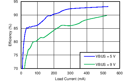
System Light Load Efficiency vs System Load Current Figure 1
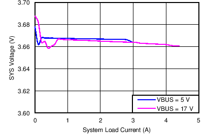
SYS Voltage Regulation vs System Load Figure 2
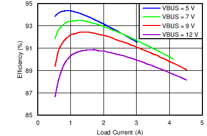
Charging Efficiency vs Charging Current Figure 3
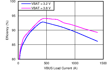
Boost Mode Efficiency vs VBUS Load Current Figure 4
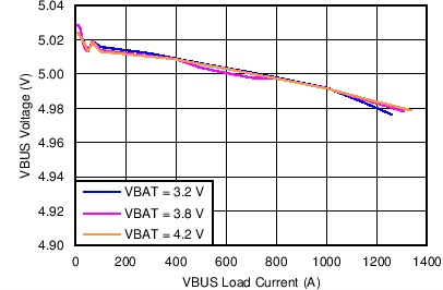
Boost Mode VBUS Voltage Regulation vs VBUS Load Current Figure 5
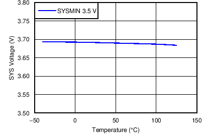
SYS Voltage vs Temperature Figure 6
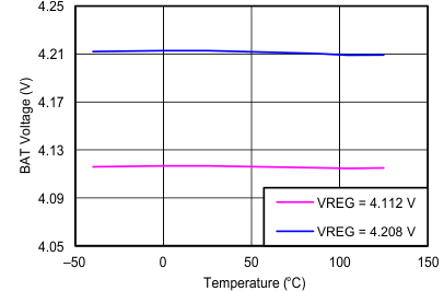
BAT Voltage vs Temperature Figure 7
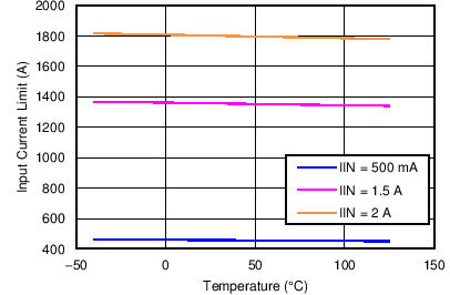
Input Current Limit vs Temperature Figure 8
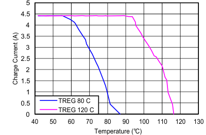
Charge Current vs Temperature Figure 9
bq24190 bq24192 bq24192I C012_SLUSAW5.png
Figure 1. System Light Load Efficiency vs System Load Current
bq24190 bq24192 bq24192I C011_SLUSAW5.png
Figure 3. Charging Efficiency vs Charging Current
bq24190 bq24192 bq24192I C005_SLUSAW5.png
Figure 5. Boost Mode VBUS Voltage Regulation vs VBUS Load Current
bq24190 bq24192 bq24192I C002A_SLUSAW5A.gif
Figure 7. BAT Voltage vs Temperature
bq24190 bq24192 bq24192I C009A_SLUSAW5A.gif
Figure 9. Charge Current vs Temperature
bq24190 bq24192 bq24192I C014_SLUSAW5.png
Figure 2. SYS Voltage Regulation vs System Load
bq24190 bq24192 bq24192I C013_SLUSAW5.png
Figure 4. Boost Mode Efficiency vs VBUS Load Current
bq24190 bq24192 bq24192I C001_SLUSAW5A.png
Figure 6. SYS Voltage vs Temperature
bq24190 bq24192 bq24192I C003_SLUSAW5A.png
Figure 8. Input Current Limit vs Temperature