ZHCSDC8A December   2014  – November 2017

PRODUCTION DATA.  

  1. 特性
  2. 应用
  3. 说明
    1.     bq24193 的 PSEL、USB On-The-Go (OTG) 和支持 JEITA 配置文件
  4. 修订历史记录
  5. 说明 (续)
  6. Pin Configuration and Functions
    1.     Pin Functions
  7. Specifications
    1. 7.1 Absolute Maximum Ratings
    2. 7.2 ESD Ratings
    3. 7.3 Recommended Operating Conditions
    4. 7.4 Thermal Information
    5. 7.5 Electrical Characteristics
    6. 7.6 Typical Characteristics
  8. Detailed Description
    1. 8.1 Overview
    2. 8.2 Functional Block Diagram
    3. 8.3 Feature Description
      1. 8.3.1 Device Power Up
        1. 8.3.1.1 Power-On-Reset (POR)
        2. 8.3.1.2 Power Up from Battery without DC Source
          1. 8.3.1.2.1 BATFET Turn Off
          2. 8.3.1.2.2 Shipping Mode
        3. 8.3.1.3 Power Up from DC Source
          1. 8.3.1.3.1 REGN LDO
          2. 8.3.1.3.2 Input Source Qualification
          3. 8.3.1.3.3 Input Current Limit Detection
          4. 8.3.1.3.4 PSEL/OTG Pins Set Input Current Limit
          5. 8.3.1.3.5 HIZ State wth 100mA USB Host
          6. 8.3.1.3.6 Force Input Current Limit Detection
        4. 8.3.1.4 Converter Power-Up
        5. 8.3.1.5 Boost Mode Operation from Battery
      2. 8.3.2 Power Path Management
        1. 8.3.2.1 Narrow VDC Architecture
        2. 8.3.2.2 Dynamic Power Management
        3. 8.3.2.3 Supplement Mode
      3. 8.3.3 Battery Charging Management
        1. 8.3.3.1 Autonomous Charging Cycle
        2. 8.3.3.2 Battery Charging Profile
        3. 8.3.3.3 Battery Path Impedance IR Compensation
        4. 8.3.3.4 Thermistor Qualification
          1. 8.3.3.4.1 JEITA Guideline Compliance
        5. 8.3.3.5 Charging Termination
          1. 8.3.3.5.1 Termination when REG02[0] = 1
          2. 8.3.3.5.2 Termination when REG05[6] = 1
        6. 8.3.3.6 Charging Safety Timer
        7. 8.3.3.7 USB Timer when Charging from USB100mA Source
      4. 8.3.4 Status Outputs (PG, STAT, and INT)
        1. 8.3.4.1 Power Good Indicator (PG)
        2. 8.3.4.2 Charging Status Indicator (STAT)
        3. 8.3.4.3 Interrupt to Host (INT)
      5. 8.3.5 Protections
        1. 8.3.5.1 Input Current Limit on ILIM
        2. 8.3.5.2 Thermal Regulation and Thermal Shutdown
        3. 8.3.5.3 Voltage and Current Monitoring in Buck Mode
          1. 8.3.5.3.1 Input Over-Voltage (ACOV)
          2. 8.3.5.3.2 System Over-Voltage Protection (SYSOVP)
        4. 8.3.5.4 Voltage and Current Monitoring in Boost Mode
          1. 8.3.5.4.1 VBUS Over-Voltage Protection
        5. 8.3.5.5 Battery Protection
          1. 8.3.5.5.1 Battery Over-Current Protection (BATOVP)
          2. 8.3.5.5.2 Charging During Battery Short Protection
          3. 8.3.5.5.3 System Over-Current Protection
      6. 8.3.6 Serial Interface
        1. 8.3.6.1 Data Validity
        2. 8.3.6.2 START and STOP Conditions
        3. 8.3.6.3 Byte Format
        4. 8.3.6.4 Acknowledge (ACK) and Not Acknowledge (NACK)
        5. 8.3.6.5 Slave Address and Data Direction Bit
          1. 8.3.6.5.1 Single Read and Write
          2. 8.3.6.5.2 Multi-Read and Multi-Write
    4. 8.4 Device Functional Modes
      1. 8.4.1 Host Mode and Default Mode
        1. 8.4.1.1 Plug in USB100mA Source with Good Battery
        2. 8.4.1.2 USB Timer when Charging from USB 100-mA Source
    5. 8.5 Register Map
      1. 8.5.1 I2C Registers
        1. 8.5.1.1  Input Source Control Register REG00 (reset = 00110000, or 30)
          1. Table 7. REG00 Input Source Control Register Description
        2. 8.5.1.2  Power-On Configuration Register REG01 (reset = 00011011, or 1B)
          1. Table 8. REG01 Power-On Configuration Register Description
        3. 8.5.1.3  Charge Current Control Register REG02 (reset = 01100000, or 60)
          1. Table 9. REG02 Charge Current Control Register Description
        4. 8.5.1.4  Pre-Charge/Termination Current Control Register REG03 (reset = 00010001, or 11)
          1. Table 10. REG03 Pre-Charge/Termination Current Control Register Description
        5. 8.5.1.5  Charge Voltage Control Register REG04 (reset = 10110010, or B2)
          1. Table 11. REG04 Charge Voltage Control Register Description
        6. 8.5.1.6  Charge Termination/Timer Control Register REG05 (reset = 10011010, or 9A)
          1. Table 12. REG05 Charge Termination/Timer Control Register Description
        7. 8.5.1.7  IR Compensation / Thermal Regulation Control Register REG06 (reset = 00000011, or 03)
          1. Table 13. REG06 IR Compensation / Thermal Regulation Control Register Description
        8. 8.5.1.8  Misc Operation Control Register REG07 (reset = 01001011, or 4B)
          1. Table 14. REG07 Misc Operation Control Register Description
        9. 8.5.1.9  System Status Register REG08
          1. Table 15. REG08 System Status Register Description
        10. 8.5.1.10 Fault Register REG09
          1. Table 16. REG09 Fault Register Description
        11. 8.5.1.11 Vender / Part / Revision Status Register REG0A (reset = 00101111, or 2F)
          1. Table 17. REG0A Vender / Part / Revision Status Register Description
  9. Application and Implementation
    1. 9.1 Application Information
    2. 9.2 Typical Application
      1. 9.2.1 Design Requirements
      2. 9.2.2 Detailed Design Procedure
        1. 9.2.2.1 Inductor Selection
        2. 9.2.2.2 Input Capacitor
        3. 9.2.2.3 Output Capacitor
      3. 9.2.3 Application Performance Plots
  10. 10Power Supply Recommendations
  11. 11Layout
    1. 11.1 Layout Guidelines
    2. 11.2 Layout Example
  12. 12器件和文档支持
    1. 12.1 文档支持
      1. 12.1.1 相关文档
    2. 12.2 接收文档更新通知
    3. 12.3 社区资源
    4. 12.4 商标
    5. 12.5 静电放电警告
    6. 12.6 Glossary
  13. 13机械、封装和可订购信息

封装选项

机械数据 (封装 | 引脚)
散热焊盘机械数据 (封装 | 引脚)
订购信息

Typical Characteristics

Table 1. Table of Figures

FIGURE NUMBER
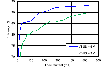
System Light Load Efficiency vs System Load Current Figure 1
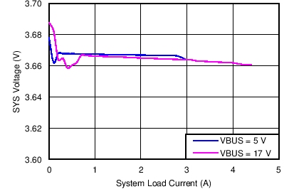
SYS Voltage Regulation vs System Load Figure 2
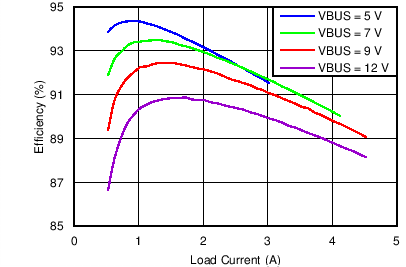
Charging Efficiency vs Charging Current Figure 3
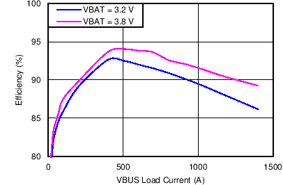
Boost Mode Efficiency vs VBUS Load Current Figure 4
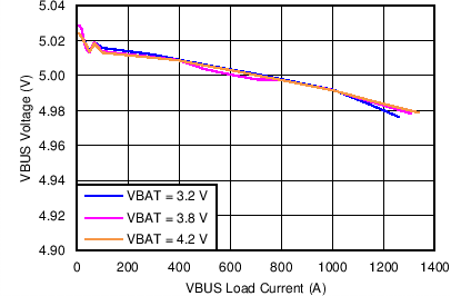
Boost Mode VBUS Voltage Regulation vs VBUS Load Current Figure 5
SYS Voltage vs Temperature Figure 6
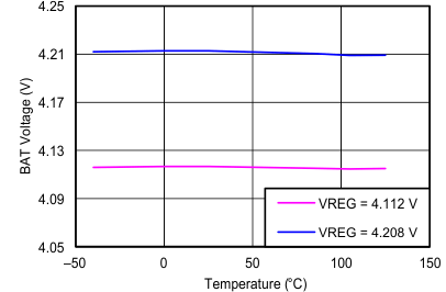
BAT Voltage vs Temperature Figure 7
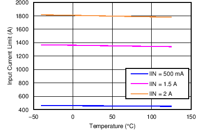
Input Current Limit vs temperature Figure 8
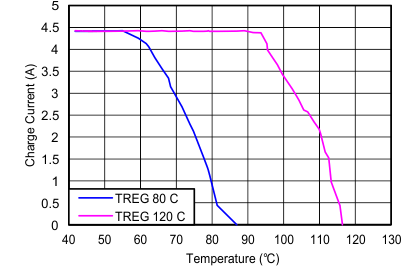
Charge Current vs temperature Figure 9
bq24193 C012_SLUSAW5.png
Figure 1. System Light Load Efficiency vs System Load Current
bq24193 C011_SLUSAW5.png
Figure 3. Charging Efficiency vs Charging Current
bq24193 C005_SLUSAW5.png
Figure 5. Boost Mode VBUS Voltage Regulation vs VBUS Load Current
bq24193 C002A_SLUSAW5A.gif
Figure 7. BAT Voltage vs Temperature
bq24193 C009A_SLUSAW5A.gif
Figure 9. Charge Current vs Temperature
bq24193 C014_SLUSAW5.png
Figure 2. SYS Voltage Regulation vs System Load
bq24193 C013_SLUSAW5.png
Figure 4. Boost Mode Efficiency vs VBUS Load Current
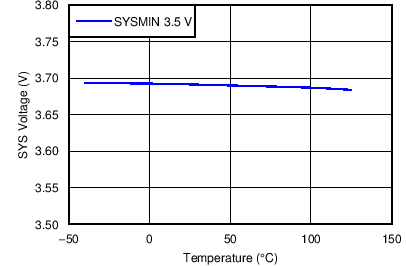
bq24193 C001_SLUSAW5A.png
Figure 6. SYS Voltage vs Temperature
bq24193 C003_SLUSAW5A.png
Figure 8. Input Current Limit vs Temperature