ZHCSBL4A September 2013 – January 2015
PRODUCTION DATA.
- 1 特性
- 2 应用
- 3 说明
- 4 修订历史记录
- 5 说明(续)
- 6 Pin Configuration and Functions
- 7 Specifications
-
8 Detailed Description
- 8.1 Overview
- 8.2 Functional Block Diagram
- 8.3
Feature Description
- 8.3.1 Device Power Up
- 8.3.2 Power Path Management
- 8.3.3 Battery Charging Management
- 8.3.4 Status Outputs (STAT, and INT)
- 8.3.5 Protections
- 8.4 Device Functional Modes
- 8.5 Programming
- 8.6
Register Map
- 8.6.1
I2C Registers
- 8.6.1.1 Input Source Control Register REG00 [reset = 01011000, or 58]
- 8.6.1.2 Power-On Configuration Register REG01 [reset = 00011011, or 0x1B]
- 8.6.1.3 Charge Current Control Register REG02 [reset = 00100000, or 0x20]
- 8.6.1.4 Pre-Charge/Termination Current Control Register REG03 [reset = 00010001, or 0x11]
- 8.6.1.5 Charge Voltage Control Register REG04 [reset = 10110010, or 0xB2]
- 8.6.1.6 Charge Termination/Timer Control Register REG05 [reset = 10011100, or 0x9C]
- 8.6.1.7 Boost Voltage/Thermal Regulation Control Register REG06 [reset = 10010011, or 0x93]
- 8.6.1.8 Misc Operation Control Register REG07 [reset = 01001011, or 4B]
- 8.6.1.9 System Status Register REG08
- 8.6.1.10 New Fault Register REG09
- 8.6.1.11 Vender / Part / Revision Status Register REG0A
- 8.6.1
I2C Registers
- 9 Application and Implementation
- 10Power Supply Recommendations
- 11Layout
- 12器件和文档支持
- 13机械封装和可订购信息
7 Specifications
7.1 Absolute Maximum Ratings(1)
| MIN | MAX | UNIT | ||
|---|---|---|---|---|
| Voltage (with respect to GND) |
VBUS (converter not switching) | –2 | 15(2) | V |
| PMID (converter not switching) | –0.3 | 15(2) | V | |
| STAT | –0.3 | 12 | V | |
| BTST | –0.3 | 12 | V | |
| SW | –2 | 7 8 (Peak for 20ns duration) |
V | |
| BAT, SYS (converter not switching) | –0.3 | 6 | V | |
| SDA, SCL, INT, OTG, ILIM, REGN, TS, QON, CE, D+, D–, | –0.3 | 7 | V | |
| BTST TO SW | –0.3 | 7 | V | |
| PGND to GND | –0.3 | 0.3 | V | |
| Output sink current | INT, STAT | 6 | mA | |
| Junction temperature | –40 | 150 | °C | |
| Storage temperature range, Tstg | –65 | 150 | °C | |
(1) Stresses beyond those listed under absolute maximum ratings may cause permanent damage to the device. These are stress ratings only, and functional operation of the device at these or any other conditions beyond those indicated under recommended operating conditions is not implied. Exposure to absolute-maximum-rated conditions for extended periods may affect device reliability. All voltage values are with respect to the network ground pin unless otherwise noted.
(2) VBUS is specified up to 16 V for a maximum of 24 hours under no load conditions.
7.2 ESD Ratings
| VALUE | UNIT | |||
|---|---|---|---|---|
| V(ESD) | Electrostatic discharge | Human body model (HBM), per ANSI/ESDA/JEDEC JS-001(1) | 1000 | V |
| Charged device model (CDM), per JEDEC specification JESD22-C101(2) | 250 | V | ||
(1) JEDEC document JEP155 states that 500-V HBM allows safe manufacturing with a standard ESD control process.
(2) JEDEC document JEP157 states that 250-V CDM allows safe manufacturing with a standard ESD control process.
7.3 Recommended Operating Conditions
| MIN | MAX | UNIT | ||
|---|---|---|---|---|
| VIN | Input voltage | 3.9 | 6.2(1) | V |
| IIN | Input current (VBUS) | 3 | A | |
| ISYS | Output current (SYS) | 3.5 | A | |
| VBAT | Battery voltage | 4.4 | V | |
| IBAT | Fast charging current | 3 | A | |
| Discharging current with internal MOSFET | 5.5 | A | ||
| TA | Operating free-air temperature range | –40 | 85 | °C |
(1) The inherent switching noise voltage spikes should not exceed the absolute maximum rating on either the BTST or SW pins. A tight layout minimizes switching noise.
7.4 Thermal Information
| THERMAL METRIC(1) | bq24295 | UNIT | |
|---|---|---|---|
| RGE (24 PIN) | |||
| RθJA | Junction-to-ambient thermal resistance | 32.2 | °C/W |
| RθJCtop | Junction-to-case (top) thermal resistance | 29.8 | |
| RθJB | Junction-to-board thermal resistance | 9.1 | |
| ψJT | Junction-to-top characterization parameter | 0.3 | |
| ψJB | Junction-to-board characterization parameter | 9.1 | |
| RθJCbot | Junction-to-case (bottom) thermal resistance | 2.2 | |
(1) For more information about traditional and new thermal metrics, see the IC Package Thermal Metrics application report, SPRA953.
7.5 Electrical Characteristics
VVBUS_UVLOZ < VVBUS < VACOV and VVBUS > VBAT + VSLEEP, TJ = –40°C to 125°C and TJ = 25°C for typical values unless other noted.| PARAMETER | TEST CONDITIONS | MIN | TYP | MAX | UNIT | |
|---|---|---|---|---|---|---|
| QUIESCENT CURRENTS | ||||||
| IBAT | Battery discharge current (BAT, SW, SYS) | VVBUS < VUVLO, VBAT = 4.2 V, leakage between BAT and VBUS | 5 | µA | ||
| High-Z Mode, or no VBUS, BATFET disabled (REG07[5] = 1), –40°C – 85°C | 16 | 20 | µA | |||
| High-Z Mode, or no VBUS, BATFET enabled (REG07[5] = 0), –40°C – 85°C | 32 | 55 | µA | |||
| IVBUS | Input supply current (VBUS) | VVBUS = 5 V, High-Z mode, No battery | 15 | 30 | µA | |
| VVBUS > VUVLO, VVBUS > VBAT, converter not switching | 1.5 | 3 | mA | |||
| VVBUS > VUVLO, VVBUS > VBAT, converter switching, VBAT = 3.2 V, ISYS = 0 A | 4 | mA | ||||
| VVBUS > VUVLO, VVBUS > VBAT, converter switching, charge disable, VBAT = 3.8 V, ISYS = 100 µA | 3.5 | mA | ||||
| IBOOST | Battery discharge current in boost mode | VBAT = 4.2 V, Boost mode, IPMID = 0 A, converter switching | 3.5 | mA | ||
| VBUS/BAT POWER UP | ||||||
| VVBUS_OP | VBUS operating voltage | 3.9 | 6.2 | V | ||
| VVBUS_UVLOZ | VBUS for active I2C, no battery | VVBUS rising | 3.6 | V | ||
| VSLEEP | Sleep mode falling threshold | VVBUS falling, VVBUS-VBAT | 35 | 80 | 120 | mV |
| VSLEEPZ | Sleep mode rising threshold | VVBUS rising, VVBUS-VBAT | 170 | 250 | 350 | mV |
| VACOV | VBUS over-voltage rising threshold | VVBUS rising | 6.2 | 6.6 | V | |
| VACOV_HYST | VBUS over-voltage falling hysteresis | VVBUS falling | 250 | mV | ||
| VBAT_UVLOZ | Battery for active I2C, no VBUS | VBAT rising | 2.3 | V | ||
| VBAT_DPL | Battery depletion threshold | VBAT falling | 2.4 | 2.6 | V | |
| VBAT_DPL_HY | Battery depletion rising hysteresis | VBAT rising | 200 | mV | ||
| VVBUSMIN | Bad adapter detection threshold | VVBUS falling | 3.8 | V | ||
| IBADSRC | Bad adapter detection current source | 30 | mA | |||
| POWER PATH MANAGEMENT | ||||||
| VSYS_MAX | Typical system regulation voltage | Isys = 0 A, BATFET (Q4) off, VBAT up to 4.2 V,
REG01[3:1] = 101, VSYSMIN = 3.5 V |
3.5 | 4.35 | V | |
| VSYS_MIN | System voltage outpu | REG01[3:1] = 101, VSYSMIN = 3.5 V | 3.5 | 3.65 | V | |
| RON(RBFET) | Top reverse blocking MOSFET on-resistance between VBUS and PMIID | 28 | 41 | mΩ | ||
| RON(HSFET) | Internal top switching MOSFET on-resistance between PMID and SW | TJ = –40°C – 85°C | 39 | 51 | mΩ | |
| TJ = -40°C – 125°C | 39 | 58 | ||||
| RON(LSFET) | Internal bottom switching MOSFET on-resistance between SW and PGND | TJ = –40°C – 85°C | 61 | 82 | mΩ | |
| TJ = -40°C – 125°C | 61 | 90 | ||||
| VFWD | BATFET forward voltage in supplement mode | BAT discharge current 10mA | 30 | mV | ||
| VSYS_BAT | SYS/BAT comparator | VSYS falling | 70 | mV | ||
| VBATGD | Battery good comparator rising threshold | VBAT rising | 3.55 | V | ||
| VBATGD_HYST | Battery good comparator falling threshold | VBAT falling | 100 | mV | ||
| BATTERY CHARGER | ||||||
| VBAT_REG_ACC | Charge voltage regulation accuracy | VBAT = 4.112 V and 4.208 V | –0.5% | 0.5% | ||
| IICHG_REG_ACC | Fast charge current regulation accuracy | VBAT = 3.8 V, ICHG = 1024 mA, TJ = 25°C | -4% | 4% | ||
| VBAT = 3.8 V, ICHG = 1024 mA, TJ = -20°C – 125°C | -7% | 7% | ||||
| VBAT = 3.8 V, ICHG = 1792 mA, TJ = -20°C – 125°C | –10% | 10% | ||||
| ICHG_20pct | Charge current with 20% option on | VBAT = 3.1 V, ICHG = 104 mA, REG02 = 03 and REG02[0] = 1 | 75 | 175 | mA | |
| VBATLOWV | Battery LOWV falling threshold | Fast charge to precharge, REG04[1] = 1 | 2.6 | 2.8 | 2.9 | V |
| VBATLOWV_HYST | Battery LOWV rising threshold | Precharge to fast charge, REG04[1] = 1 (Typical 200-mV hysteresis) |
2.8 | 3.0 | 3.1 | V |
| IPRECHG_ACC | Precharge current regulation accuracy | VBAT = 2.6 V, ICHG = 256 mA | –20% | 20% | ||
| ITYP_TERM_ACC | Typical termination current | ITERM = 256 mA, ICHG = 2048 mA | 265 | mA | ||
| ITERM_ACC | Termination current accuracy | ITERM = 256 mA, ICHG = 2048 mA | –22.5% | 22.5% | ||
| VSHORT | Battery short voltage | VBAT falling | 2.0 | V | ||
| VSHORT_HYST | Battery Short Voltage hysteresis | VBAT rising | 200 | mV | ||
| ISHORT | Battery short current | VBAT < 2.2 V | 100 | mA | ||
| VRECHG | Recharge threshold below VBAT_REG | VBAT falling, REG04[0] = 0 | 100 | mV | ||
| tRECHG | Recharge deglitch time | VBAT falling, REG04[0] = 0 | 20 | ms | ||
| RON_BATFET | SYS-BAT MOSFET on-resistance | TJ = 25°C | 24 | 28 | mΩ | |
| TJ = –40°C – 125°C | 24 | 35 | ||||
| INPUT VOLTAGE/CURRENT REGULATION | ||||||
| VINDPM_REG_ACC | Input voltage regulation accuracy | -2% | 2% | |||
| IUSB_DPM | USB Input current regulation limit, VBUS = 5V, current pulled from SW | USB100 | 85 | 100 | mA | |
| USB150 | 125 | 150 | mA | |||
| USB500 | 440 | 500 | mA | |||
| USB900 | 750 | 900 | mA | |||
| IADPT_DPM | Input current regulation accuracy | IADP = 1.5 A, REG00[2:0] = 101 | 1.3 | 1.5 | A | |
| IIN_START | Input current limit during system start up | VSYS < 2.2 V | 100 | mA | ||
| KILIM | IIN = KILIM/RILIM | IINDPM = 1.5 A | 395 | 435 | 475 | A x Ω |
| D+/D- DETECTION | ||||||
| VD+_SRC | D+ voltage source | 0.5 | 0.7 | V | ||
| ID+_SRC | D+ connection check current source | 7 | 14 | µA | ||
| ID–_SINK | D– current sink | 50 | 100 | 150 | µA | |
| ID_LKG | Leakage current into D+/D– | D–, switch open | –1 | 1 | µA | |
| D+, switch open | –1 | 1 | µA | |||
| VD+_LOW | D+ low comparator threshold | 0.8 | V | |||
| VD–_LOWdatref | D– low comparator threshold | 250 | 400 | mV | ||
| RD–_DWN | D– pulldown for connection check | 14.25 | 24.8 | kΩ | ||
| tSDP_DEFAULT | Charging timer with 100mA USB host in default mode | 45 | mins | |||
| Vadpt1_lo | D+ low comparator threshold for non-standard adapter Divider-1 | As percentage of REGN, 0°C – 85°C(1) | 46.5% | 48% | 49.5% | |
| Vadpt1_hi | D+ low comparator threshold for non-standard adapter divider-1 | As percentage of REGN, 0°C – 85°C(1) | 58.5% | 60% | 61.5% | |
| Vadpt2_lo | D+ low comparator threshold for non-standard adapter divider-2 | As percentage of REGN, 0°C – 85°C(1) | 15.5% | 17% | 18.5% | |
| Vadpt2_hi | D+ low comparator threshold for Non-standard adapter divider-2 | As percentage of REGN, 0°C – 85°C(1) | 28.5% | 30% | 31.5% | |
| Vadpt3_lo | D- low comparator threshold for non-standard adapter divider-3 | As percentage of REGN, 0°C – 85°C(1) | 46.5% | 48% | 49.5% | |
| Vadpt3_hi | D- high comparator threshold for non-standard adapter divider-3 | As percentage of REGN, 0°C – 85°C(1) | 58.5% | 60% | 61.5% | |
| BAT OVER-VOLTAGE PROTECTION | ||||||
| VBATOVP | Battery over-voltage threshold | VBAT rising, as percentage of VBAT_REG | 104% | |||
| VBATOVP_HYST | Battery over-voltage hysteresis | VBAT falling, as percentage of VBAT_REG | 2% | |||
| tBATOVP | Battery over-voltage deglitch time to disable charge | 1 | µs | |||
| THERMAL REGULATION AND THERMAL SHUTDOWN | ||||||
| TJunction_REG | Junction temperature regulation accuracy | REG06[1:0] = 11 | 120 | °C | ||
| TSHUT | Thermal shutdown rising temperature | Temperature increasing | 160 | °C | ||
| TSHUT_HYS | Thermal shutdown hysteresis | 30 | °C | |||
| Thermal shutdown rising deglitch | Temperature increasing delay | 1 | ms | |||
| Thermal shutdown falling deglitch | Temperature decreasing delay | 1 | ms | |||
| COLD/HOT THERMISTER COMPARATOR | ||||||
| VLTF | Cold temperature threshold, TS pin voltage rising threshold | Charger suspends charge. as percentage to VREGN | 73% | 73.5% | 74% | |
| VLTF_HYS | Cold temperature hysteresis, TS pin voltage falling | As percentage to VREGN | 0.4% | |||
| VHTF | Hot temperature TS pin voltage rising threshold | As percentage to VREGN | 46.6% | 47.2% | 48.8% | |
| VTCO | Cut-off temperature TS pin voltage falling threshold | As percentage to VREGN | 44.2% | 44.7% | 45.2% | |
| Deglitch time for temperature out of range detection | VTS > VLTF, or VTS < VTCO, or VTS < VHTF | 10 | ms | |||
| VBCOLD0 | Cold temperature threshold, TS pin voltage rising threshold | As percentage to VREGN REG02[1] = 0 (Approx. -10°C w/ 103AT) |
75.5% | 76% | 76.5% | |
| VBCOLD0_HYS | As percentage to VREGN REG02[1] = 0 (Approx. 1°C w/ 103AT) |
1% | ||||
| VBCOLD1 | Cold temperature threshold 1, TS pin voltage rising threshold | As percentage to VREGN REG02[1] = 1 (Approx. -20°C w/ 103AT) |
78.5% | 79% | 79.5% | |
| VBCOLD1_HYS | As percentage to VREGN REG02[1] = 1 (Approx. 1°C w/ 103AT) |
1% | ||||
| VBHOT0 | Hot temperature threshold, TS pin voltage falling threshold | As percentage to VREGN REG06[3:2] = 01 (Approx. 55°C w/ 103AT) |
35.5% | 36% | 36.5% | |
| VBHOT0_HYS | As percentage to VREGN REG06[3:2] = 01 (Approx. 3°C w/ 103AT) |
3% | ||||
| VBHOT1 | Hot temperature threshold 1, TS pin voltage falling threshold | As percentage to VREGN REG06[3:2] = 00 (Approx. 60°C w/ 103AT) |
32.5% | 33% | 33.5% | |
| VBHOT1_HYS | As percentage to VREGN REG06[3:2] = 00 (Approx. 3°C w/ 103AT) |
3% | ||||
| VBHOT2 | Hot temperature threshold 2, TS pin voltage falling threshold | As percentage to VREGN REG06[3:2] = 10 (Approx. 65°C w/ 103AT) |
29.5% | 30% | 30.5% | |
| VBHOT2_HYS | As percentage to VREGN REG06[3:2] = 10 (Approx. 3°C w/ 103AT) |
3% | ||||
| CHARGE OVER-CURRENT COMPARATOR | ||||||
| IHSFET_OCP | HSFET cycle by cycle over-current threshold | 5.3 | 7.5 | A | ||
| IBATFET_OCP | System over load threshold | 5.5 | 6.6 | A | ||
| VLSFET_UCP | LSFET charge under-current falling threshold | From sync mode to non-sync mode | 100 | mA | ||
| FSW | PWM Switching frequency, and digital clock | 1300 | 1500 | 1700 | kHz | |
| DMAX | Maximum PWM duty cycle | 97% | ||||
| VBTST_REFRESH | Bootstrap refresh comparator threshold | VBTST-VSW when LSFET refresh pulse is requested, VBUS = 5 V | 3.6 | V | ||
| BOOST MODE OPERATION | ||||||
| VOTG_REG | Boost mode output voltage | I(PMID) = 0, REG06[7:4] = 1001 (5.126 V) | 5.12 | V | ||
| VOTG_REG_ACC | Boost mode output voltage accuracy | I(PMID) = 0, REG06[7:4] = 1001 (5.126 V) | -3% | 3% | ||
| VOTG_BAT | Battery voltage exiting boost mode | BAT falling, REG04[1] = 1 | 2.9 | V | ||
| IOTG | Boost mode output current on PMID | 1.3 | A | |||
| VOTG_OVP | OTG over-voltage threshold | Rising threshold | 5.8 | 6 | V | |
| VOTG_OVP_HYS | OTG over-voltage threshold hysteresis | Falling threshold | 300 | mV | ||
| IOTG_LSOCP | LSFET cycle by cycle current limit | 5 | A | |||
| IOTG_HSZCP | HSFET under current falling threshold | 100 | mA | |||
| REGN LDO | ||||||
| VREGN | REGN LDO output voltage | VVBUS = 6 V, IREGN = 40 mA | 4.8 | 5 | 5.5 | V |
| VVBUS = 5 V, IREGN = 20 mA | 4.7 | 4.8 | V | |||
| IREGN | REGN LDO current limit | VVBUS = 5 V, VREGN = 3.8 V | 50 | mA | ||
| LOGIC I/O PIN CHARACTERISTICS (OTG, CE, STAT, QON) | ||||||
| VILO | Input low threshold | 0.4 | V | |||
| VIH | Input high threshold (CE, STAT, QON) | 1.3 | V | |||
| VIH_OTG | Input high threshold (OTG) | 1.1 | V | |||
| VOUT_LO | Output low saturation voltage | Sink current = 5 mA | 0.4 | V | ||
| IBIAS | High level leakage current (OTG, CE, STAT ) | Pull-up rail 1.8 V | 1 | µA | ||
| IBIAS | High level leakage current (QON) | Pull-up rail 3.6 V | 8 | µA | ||
| I2C INTERFACE (SDA, SCL, INT) | ||||||
| VIH | Input high threshold level | VPULL-UP = 1.8 V, SDA and SCL | 1.3 | V | ||
| VIL | Input low threshold level | VPULL-UP = 1.8 V, SDA and SCL | 0.4 | V | ||
| VOL | Output low threshold level | Sink current = 5 mA | 0.4 | V | ||
| IBIAS | High-level leakage current | VPULL-UP = 1.8 V, SDA and SCL | 1 | µA | ||
| fSCL | SCL clock frequency | 400 | kHz | |||
| DIGITAL CLOCK AND WATCHDOG TIMER | ||||||
| fHIZ | Digital crude clock | REGN LDO disabled | 15 | 35 | 50 | kHz |
| fDIG | Digital clock | REGN LDO enabled | 1300 | 1500 | 1700 | kHz |
(1) REGN LDO is configured in drop-out mode. VBUS is close to REGN when IREGN = 0 mA.
7.6 Timing Requirements
| MIN | TYP | MAX | UNIT | |||
|---|---|---|---|---|---|---|
| VBUS/BAT POWER UP | ||||||
| tBADSRC | Bad source detection duration | 30 | ms | |||
| QON TIMING | ||||||
| tQON | QON pin high time to turn on BATFET | 2 | ms | |||
| DIGITAL CLOCK AND WATCHDOG TIMER | ||||||
| tWDT | REG05[5:4] = 11 | REGN LDO disabled | 112 | 160 | sec | |
| REGN LDO enabled | 136 | 160 | ||||
 Figure 1. I2C-Compatible Interface Timing Diagram
7.7 Typical Characteristics
Table 1. Table of Figures
| FIGURE | |
|---|---|
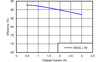
| Charging Efficiency vs Charging Current (DCR = 10 mΩ) | Figure 2 |
| System Efficiency vs System Load Current (DCR = 10 mΩ) | Figure 3 |
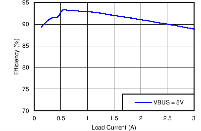
| Boost Mode Efficiency vs VBUS Load Current (DCR = 10 mΩ) | Figure 4 |
| SYS Voltage Regulation vs System Load Current | Figure 5 |
| Boost Mode PMID Voltage Regulation (Typical Output = 5.126 V, REG06[7:4] = 1001) vs PMID Load Current | Figure 6 |
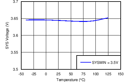
| SYS Voltage vs Temperature | Figure 7 |
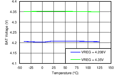
| BAT Voltage vs Temperature | Figure 8 |
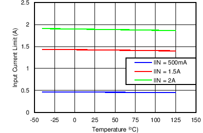
| Input Current Limit vs Temperature | Figure 9 |
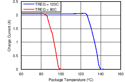
| Charge Current vs Package Temperature | Figure 10 |
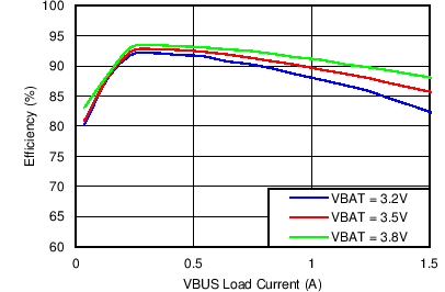
vs VBUS Load Current
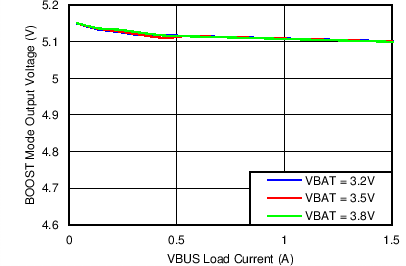
| Typical Output = 5.126 V, REG06[7:4] = 1001 | ||
vs System Load Current
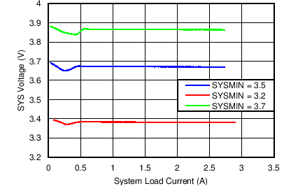
vs System Load Current
