ZHCSKL0D December   2009  – December 2019 BQ24610 , BQ24617

PRODUCTION DATA.  

  1. 特性
  2. 应用
  3. 说明
    1.     Device Images
      1.      简化原理图
  4. 修订历史记录
  5. 说明 (续)
  6. Device Comparison Table
  7. Pin Configuration and Functions
    1.     Pin Functions
  8. Specifications
    1. 8.1 Absolute Maximum Ratings
    2. 8.2 ESD Ratings
    3. 8.3 Recommended Operating Conditions
    4. 8.4 Thermal Information
    5. 8.5 Electrical Characteristics
    6. 8.6 Typical Characteristics
  9. Detailed Description
    1. 9.1 Overview
    2. 9.2 Functional Block Diagram
    3. 9.3 Feature Description
      1. 9.3.1  Battery Voltage Regulation
      2. 9.3.2  Battery Current Regulation
      3. 9.3.3  Input Adapter Current Regulation
      4. 9.3.4  Precharge
      5. 9.3.5  Charge Termination, Recharge, and Safety Timer
      6. 9.3.6  Power Up
      7. 9.3.7  Enable and Disable Charging
      8. 9.3.8  System Power Selector
      9. 9.3.9  Automatic Internal Soft-Start Charger Current
      10. 9.3.10 Converter Operation
      11. 9.3.11 Synchronous and Nonsynchronous Operation
      12. 9.3.12 Cycle-by-Cycle Charge Undercurrent Protection
      13. 9.3.13 Input Overvoltage Protection (ACOV)
      14. 9.3.14 Input Undervoltage Lockout (UVLO)
      15. 9.3.15 Battery Overvoltage Protection
      16. 9.3.16 Cycle-by-Cycle Charge Overcurrent Protection
      17. 9.3.17 Thermal Shutdown Protection
      18. 9.3.18 Temperature Qualification
      19. 9.3.19 Timer Fault Recovery
      20. 9.3.20 PG Output
      21. 9.3.21 CE (Charge Enable)
      22. 9.3.22 Charge Status Outputs
      23. 9.3.23 Battery Detection
    4. 9.4 Device Functional Modes
  10. 10Application and Implementation
    1. 10.1 Application Information
    2. 10.2 Typical Applications
      1. 10.2.1 System with Power Path
        1. 10.2.1.1 Design Requirements
        2. 10.2.1.2 Detailed Design Procedure
          1. 10.2.1.2.1 Inductor Selection
          2. 10.2.1.2.2 Input Capacitor
          3. 10.2.1.2.3 Output Capacitor
          4. 10.2.1.2.4 Power MOSFETs Selection
          5. 10.2.1.2.5 Input Filter Design
          6. 10.2.1.2.6 Inductor, Capacitor, and Sense Resistor Selection Guidelines
        3. 10.2.1.3 Application Curves
      2. 10.2.2 Simplified System without Power Path or DPM
        1. 10.2.2.1 Design Requirements
        2. 10.2.2.2 Detailed Design Procedure
        3. 10.2.2.3 Application Curves
      3. 10.2.3 Lead-Acid Charging System
        1. 10.2.3.1 Design Requirements
        2. 10.2.3.2 Detailed Design Procedure
        3. 10.2.3.3 Application Curves
  11. 11Power Supply Recommendations
  12. 12Layout
    1. 12.1 Layout Guidelines
    2. 12.2 Layout Example
  13. 13器件和文档支持
    1. 13.1 器件支持
      1. 13.1.1 第三方米6体育平台手机版_好二三四免责声明
    2. 13.2 相关链接
    3. 13.3 接收文档更新通知
    4. 13.4 支持资源
    5. 13.5 商标
    6. 13.6 静电放电警告
    7. 13.7 Glossary
  14. 14机械、封装和可订购信息

封装选项

机械数据 (封装 | 引脚)
散热焊盘机械数据 (封装 | 引脚)
订购信息

Typical Characteristics

Table 1. Table of Graphs

FIGURE
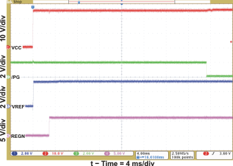
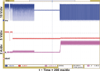
REF REGN and PG Power Up (CE = 1) Figure 1
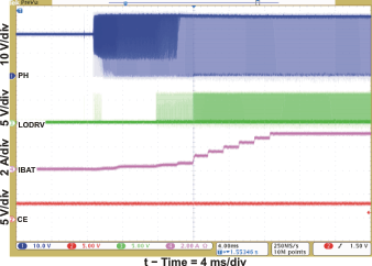
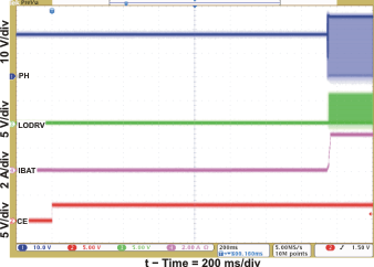
Charge Enable Figure 2
Current Soft Start (CE = 1) Figure 3
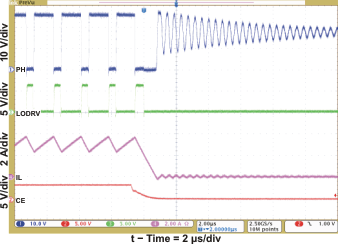
Charge Disable Figure 4
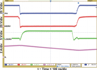
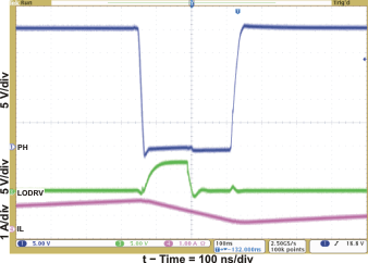
Continuous Conduction Mode Switching Waveforms Figure 5
Cycle-by-Cycle Synchronous to Nonsynchronous Figure 6
100% Duty and Refresh Pulse Figure 7
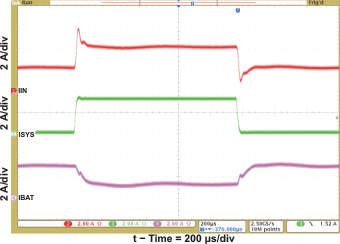
Transient System Load (DPM) Figure 8
Battery Insertion Figure 9
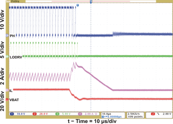
Battery-to-Ground Short Protection Figure 10
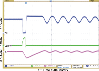
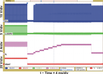
Battery-to-Ground Short Transition Figure 11
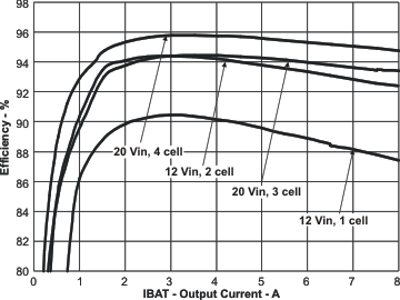
Efficiency vs Output Current Figure 12
BQ24610 BQ24617 ref_rgn_lus892.gif
Figure 1. REF REGN and PG Power Up (CE = 1)
BQ24610 BQ24617 cur_sfst_lus892.gif
Figure 3. Current Soft Start (CE = 1)
BQ24610 BQ24617 cc_mode_lus892.gif
Figure 5. Continuous Conduction Mode Switching Waveforms
BQ24610 BQ24617 duty_fresh_lus892.gif
Figure 7. 100% Duty and Refresh Pulse
BQ24610 BQ24617 ins_batt_lus892.gif
Figure 9. Battery Insertion
BQ24610 BQ24617 short_trans_lus892.gif
Figure 11. Battery-to-GND Short Transition
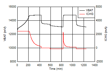
BQ24610 BQ24617 D0001.gif
Figure 13. Lead Acid Charging Profile
BQ24610 BQ24617 chg_enab_lus892.gif
Figure 2. Charge Enable
BQ24610 BQ24617 chg_dis_lus892.gif
Figure 4. Charge Disable
BQ24610 BQ24617 cycle_lus892.gif
Figure 6. Cycle-by-Cycle Synchronous to Nonsynchronous
BQ24610 BQ24617 trans_sys_lus892.gif
Figure 8. Transient System Load (DPM)
BQ24610 BQ24617 short_pro_lus892.gif
Figure 10. Battery-to-GND Short Protection
BQ24610 BQ24617 eff_comb_lus892.gif
Figure 12. Efficiency vs Output Current