ZHCSKL0D December 2009 – December 2019 BQ24610 , BQ24617
PRODUCTION DATA.
- 1 特性
- 2 应用
- 3 说明
- 4 修订历史记录
- 5 说明 (续)
- 6 Device Comparison Table
- 7 Pin Configuration and Functions
- 8 Specifications
-
9 Detailed Description
- 9.1 Overview
- 9.2 Functional Block Diagram
- 9.3
Feature Description
- 9.3.1 Battery Voltage Regulation
- 9.3.2 Battery Current Regulation
- 9.3.3 Input Adapter Current Regulation
- 9.3.4 Precharge
- 9.3.5 Charge Termination, Recharge, and Safety Timer
- 9.3.6 Power Up
- 9.3.7 Enable and Disable Charging
- 9.3.8 System Power Selector
- 9.3.9 Automatic Internal Soft-Start Charger Current
- 9.3.10 Converter Operation
- 9.3.11 Synchronous and Nonsynchronous Operation
- 9.3.12 Cycle-by-Cycle Charge Undercurrent Protection
- 9.3.13 Input Overvoltage Protection (ACOV)
- 9.3.14 Input Undervoltage Lockout (UVLO)
- 9.3.15 Battery Overvoltage Protection
- 9.3.16 Cycle-by-Cycle Charge Overcurrent Protection
- 9.3.17 Thermal Shutdown Protection
- 9.3.18 Temperature Qualification
- 9.3.19 Timer Fault Recovery
- 9.3.20 PG Output
- 9.3.21 CE (Charge Enable)
- 9.3.22 Charge Status Outputs
- 9.3.23 Battery Detection
- 9.4 Device Functional Modes
- 10Application and Implementation
- 11Power Supply Recommendations
- 12Layout
- 13器件和文档支持
- 14机械、封装和可订购信息
封装选项
机械数据 (封装 | 引脚)
- RGE|24
散热焊盘机械数据 (封装 | 引脚)
- RGE|24
订购信息
9.3.23 Battery Detection
For applications with removable battery packs, BQ2461x provides a battery-absent detection scheme to reliably detect insertion or removal of battery packs.
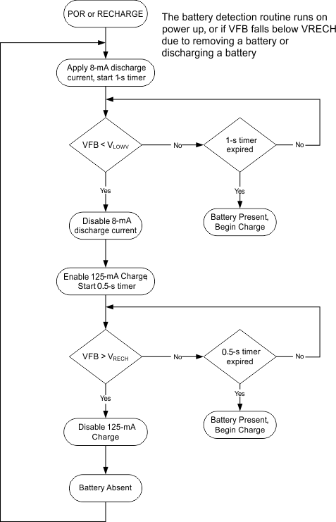
 Figure 17. Battery Detection Flow Chart
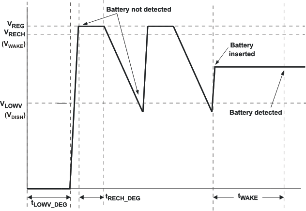
 Once the device has powered up, an 8-mA discharge current is applied to the SRN terminal. If the battery voltage falls below the LOWV threshold within 1 second, the discharge source is turned off, and the charger is turned on at low charge current (125 mA). If the battery voltage rises above the recharge threshold within 500 ms, there is no battery present and the cycle restarts. If either the 500-ms or 1-second timer times out before its respective threshold is hit, a battery is detected and a charge cycle is initiated.
 Figure 18. Battery Detect Timing Diagram
 Ensure that the total output capacitance at the battery node is not so large that the discharge current source cannot pull the voltage below the LOWV threshold during the 1-second discharge time. The maximum output capacitance can be calculated as follows:

where
- CMAX is the maximum output capacitance.
- IDISCH is the discharge current.
- tDISCH is the discharge time.
- R2 and R1 are the voltage feedback resistors from the battery to the VFB pin.
The 0.5 factor is the difference between the RECHARGE and the LOWV thresholds at the VFB pin.
Example
For a 3-cell Li+ charger, with R2 = 500 kΩ, R1 = 100 kΩ (giving 12.6 V for voltage regulation), IDISCH = 8 mA, tDISCH = 1 second,

Based on these calculations, no more than 2.7 mF should be allowed on the battery node for proper operation of the battery detection circuit.