SLUSA44A March 2010 – July 2015
PRODUCTION DATA.
- 1 Features
- 2 Applications
- 3 Description
- 4 Revision History
- 5 Pin Configuration and Functions
- 6 Specifications
-
7 Detailed Description
- 7.1 Overview
- 7.2 Functional Block Diagram
- 7.3
Feature Description
- 7.3.1 Output Voltage Regulation
- 7.3.2 Output Current Regulation
- 7.3.3 Power Up
- 7.3.4 Enable and Disable Charging
- 7.3.5 Automatic Internal Soft-Start Charger Current
- 7.3.6 Converter Operation
- 7.3.7 Synchronous and Nonsynchronous Operation
- 7.3.8 Input Overvoltage Protection (ACOV)
- 7.3.9 Output Overvoltage Protection
- 7.3.10 Cycle-by-Cycle Charge Overcurrent Protection
- 7.3.11 Thermal Shutdown Protection
- 7.3.12 Temperature Qualification
- 7.3.13 CE (Charge Enable)
- 7.3.14 PG Output
- 7.3.15 Charge Status Outputs
- 7.4 Device Functional Modes
- 8 Application and Implementation
- 9 Power Supply Recommendations
- 10Layout
- 11Device and Documentation Support
- 12Mechanical, Packaging, and Orderable Information
7 Detailed Description
7.1 Overview
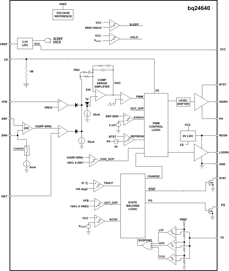
The bq24640 device is a stand-alone, integrated super capacitor charger. The device employs a switched-mode synchronous buck PWM controller with constant switching frequency.
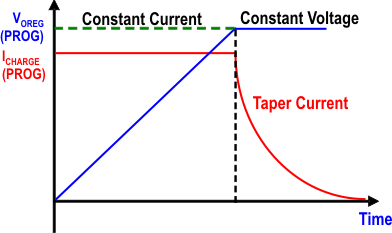
Charging begins in one of two phases (depending upon super capacitor voltage): constant current (fast-charge current regulation), and constant voltage (fast-charge voltage regulation). Constant current can be configured through the ISET pin, allowing for flexibility in the super capacitor charging profile. During charging, the integrated fault monitors of the device, such as output overvoltage protection (VOV_RISE), thermal shutdown (internal TSHUT and TS pin), and input voltage protection (VACOV and VUVLO), ensure super capacitor safety.
The bq24640 has two status pins (STAT and PG) to indicate the charging status and input voltage (AC adapter) status. These pins can be used to drive LEDs or communicate with a host processor.
 Figure 8. Typical Charging Profile
7.2 Functional Block Diagram

7.3 Feature Description
7.3.1 Output Voltage Regulation
The bq24640 uses a high-accuracy voltage regulator for the charging voltage. The charge voltage is programmed through a resistor-divider from the output to ground, with the midpoint tied to the VFB pin. The voltage at the VFB pin is regulated to 2.1 V, giving Equation 1 for the regulation voltage:

where
- R2 is connected from VFB to the output, and R1 is connected from VFB to GND.
7.3.2 Output Current Regulation
The ISET input sets the maximum charging current. Output current is sensed by resistor RSR connected between SRP and SRN. The full-scale differential voltage between SRP and SRN is 100 mV. Thus, for a 10-mΩ sense resistor, the maximum charging current is 10 A. The equation for charge current is:

The input voltage range of ISET is from 0 V to 2 V. The SRP and SRN pins are used to sense voltage across RSR with default value of 10 mΩ. However, resistors of other values can also be used. A larger sense resistor will give a larger sense voltage and a higher regulation accuracy, but this comes at the expense of higher conduction loss.
7.3.3 Power Up
The bq24640 uses a sleep comparator to determine if the source of power on the VCC pin is a valid supply to charge the capacitor. If the VCC voltage is above the UVLO threshold and greater than the SRN voltage, and all other conditions are met, bq24640 will then start to charge (see Enable and Disable Charging). If the SRN voltage is greater than VCC, the bq24640 enters a low quiescent current sleep mode to minimize current drain from the capacitor (<15 µA).
If VCC is below the UVLO threshold, the device is disabled.
7.3.4 Enable and Disable Charging
The following conditions have to be valid before charge is enabled:
- CE is HIGH.
- The device is not in undervoltage lockout (UVLO) mode and not in VCCLOWV.
- The device is not in sleep mode (that is, VCC > SRN).
- The VCC voltage is lower than the AC overvoltage threshold (VCC < VACOV).
- 30-ms delay is complete after initial power up.
- The REGN LDO and VREF LDO voltages are at the correct levels.
- Thermal shutdown (TSHUT) is not valid.
- TS fault is not detected.
One of the following conditions will stop ongoing charging:
- CE is LOW.
- Adapter is removed, thus causing the device to enter VCCLOWV.
- The device is in sleep mode (that is, VCC < SRN).
- Adapter is over voltage.
- The REGN or VREF LDOs voltage are not valid.
- TSHUT IC temperature threshold is reached.
- TS voltage goes out of range indicating the temperature is too hot or too cold.
7.3.5 Automatic Internal Soft-Start Charger Current
The charger automatically soft starts the charger regulation current to ensure there is no overshoot or stress on the output capacitor. The soft start consists of stepping up the charge regulation current into 8 evenly divided steps up to the programmed charge current. Each step lasts around 1.6 ms, for a typical rise time of 13 ms. No external components are needed for this function.
7.3.6 Converter Operation
The synchronous buck PWM converter uses a fixed-frequency voltage mode with feed-forward control scheme. A type III compensation network allows using ceramic capacitors at the output of the converter. The compensation input stage is connected internally between the feedback output (FBO) and the error amplifier input (EAI). The feedback compensation stage is connected between the error amplifier input (EAI) and error amplifier output (EAO). The LC output filter is selected to give a resonant frequency of 12 kHz to 17 kHz, where resonant frequency, fo, is given by:

An internal saw-tooth ramp is compared to the internal EAO error control signal to vary the duty-cycle of the converter. The ramp height is 7% of the input adapter voltage making it always directly proportional to the input adapter voltage. This cancels out any loop gain variation due to a change in input voltage, and simplifies the loop compensation. The ramp is offset in order to allow zero percent duty-cycle when the EAO signal is below the ramp. The EAO signal is also allowed to exceed the saw-tooth ramp signal in order to get a 100% duty-cycle PWM request. Internal gate drive logic allows achieving 99.98% duty-cycle while ensuring the N-channel upper device always has enough voltage to stay fully on. If the BTST pin to PH pin voltage falls below 4.2 V for more than 3 cycles, then the high-side N-channel power MOSFET is turned off and the low-side N-channel power MOSFET is turned on to pull the PH node down and recharge the BTST capacitor. Then the high-side driver returns to 100% duty-cycle operation until the (BTST-PH) voltage is detected to fall low again due to leakage current discharging the BTST capacitor below the 4.2 V, and the reset pulse is issued.
The fixed-frequency oscillator keeps tight control of the switching frequency under all conditions of input voltage, output voltage, charge current, and temperature, simplifying output filter design and keeping it out of the audible noise region.
7.3.7 Synchronous and Nonsynchronous Operation
The charger operates in synchronous mode when the SRP-SRN voltage is above 5 mV (0.5-A inductor current for a 10-mΩ sense resistor). During synchronous mode, the internal gate drive logic ensures there is break-before-make complimentary switching to prevent shoot-through currents. During the 30-ns dead time where both FETs are off, the body-diode of the low-side power MOSFET conducts the inductor current. Having the low-side FET turnon keeps the power dissipation low, and allows safely charging at high currents. During synchronous mode the inductor current is always flowing and converter operates in continuous conduction mode (CCM), creating a fixed two-pole system.
The charger operates in nonsynchronous mode when the SRP-SRN voltage is below 5 mV (0.5-A inductor current on 10-mΩ sense resistor). The charger is forced into nonsynchronous mode when the super capacitor voltage is lower than 2 V or when the average SRP-SRN voltage is lower than 1.25 mV (125 mA on 10-mΩ sense resistor).
During nonsynchronous operation, the body-diode of lower-side MOSFET can conduct the positive inductor current after the high-side N-channel power MOSFET turns off. When the load current decreases and the inductor current drops to zero, the body diode will be naturally turned off and the inductor current will become discontinuous. This mode is called Discontinuous Conduction Mode (DCM). During DCM, the low-side N-channel power MOSFET will turn on when the bootstrap capacitor voltage drops below 4.2 V, then the low-side power MOSFET will turn off and stay off until the beginning of the next cycle, where the high-side power MOSFET is turned on again. The low-side MOSFET on-time is required to ensure the bootstrap capacitor is always recharged and able to keep the high-side power MOSFET on during the next cycle.
At very low currents during nonsynchronous operation, there may be a small amount of negative inductor current during the recharge pulse. The charge must be low enough to be absorbed by the input capacitance. Whenever the converter goes into zero percent duty-cycle, the high-side MOSFET does not turn on, and the low-side MOSFET does not turn on (only recharge pulse) either, and there is almost no discharge from the output.
During the DCM mode the loop response automatically changes and has a single-pole system at which the pole is proportional to the load current, because the converter does not sink current, and only the load provides a current sink. This means at very low currents the loop response is slower, as there is less sinking current available to discharge the output voltage.
7.3.8 Input Overvoltage Protection (ACOV)
ACOV provides protection to prevent system damage due to high input voltage. When the adapter voltage reaches the ACOV threshold, charge is disabled.
7.3.9 Output Overvoltage Protection
The converter will not allow the high-side FET to turn-on until the output voltage goes below 102% of the regulation voltage. This allows one-cycle response to an overvoltage condition – such as occurs when the load is removed. An 8-mA current sink from SRP-SRN to GND is on during charge and allows discharging the output capacitors.
7.3.10 Cycle-by-Cycle Charge Overcurrent Protection
The charger has a secondary cycle-to-cycle overcurrent protection. The charger monitors the charge current, and prevents the current from exceeding 160% of the programmed charge current. The high-side gate drive turns off when the overcurrent is detected, and automatically resumes when the current falls below the overcurrent threshold.
7.3.11 Thermal Shutdown Protection
The VQFN package has low thermal impedance, which provides good thermal conduction from the silicon to the ambient, to keep junctions temperatures low. As added level of protection, the charger converter turns off and self-protects whenever the junction temperature exceeds the TSHUT threshold of 145°C. The charger stays off until the junction temperature falls below 130°C.
7.3.12 Temperature Qualification
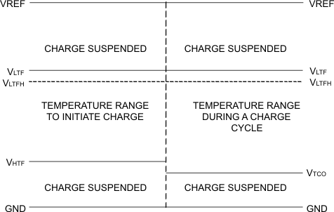
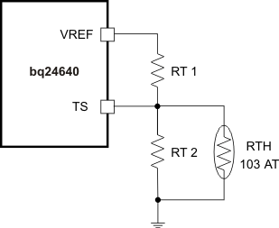
The controller continuously monitors load temperature by measuring the voltage between the TS pin and GND. A negative temperature coefficient thermistor (NTC) and an external voltage divider typically develop this voltage. The controller compares this voltage against its internal thresholds to determine if charging is allowed. To initiate a charge cycle, the temperature must be within the V(LTF) to V(HTF) thresholds. If temperature is outside of this range, the controller suspends charge and waits until the temperature is within the V(LTF) to V(HTF) range. During the charge cycle the temperature must be within the V(LTF) to V(TCO) thresholds. If temperature is outside of this range, the controller suspends charge and waits until the temperature is within the V(LTF) to V(HTF) range. The controller suspends charge by turning off the PWM charge FETs. If the TS function is not required, R9 and R10 can be the same value so the voltage on TS is 1.65 V with VREF as the reference supply.
 Figure 9. TS Pin, Thermistor Sense Thresholds
Assuming a 103AT NTC thermistor is selector, the value RT1 and RT2 can be determined by using the following equations:


 Figure 10. TS Resistor Network
7.3.13 CE (Charge Enable)
The CE digital input is used to disable or enable the charge process. A high-level signal on this pin enables charge, provided all the other conditions for charge are met (see Enabling and Disabling Charge). A high-to-low transition on this pin also resets all timers and fault conditions. There is an internal 1-MΩ pulldown resistor on the CE pin, so if CE is floated the charge will not turn on.
7.3.14 PG Output
The open-drain PG (power good) output indicates when the VCC voltage is present. The open-drain FET turns on whenever bq24640 is not in UVLO mode and not in sleep mode (that is, V(VCC) > V(SRN) and V(VCC) > V(UVLO)). The PG pin can be used to drive an LED or communicate to the host processor.
7.3.15 Charge Status Outputs
The open-drain STAT output indicates various charger operations as shown in Table 2. These status pins can be used to drive LEDs or communicate with the host processor.
NOTE
OFF indicates that the open-drain transistor is turned off.
Table 2. STAT Pin Definition
| CHARGE STATE | STAT |
|---|---|
| CE high | ON |
| Sleep mode | OFF |
| Charge Suspend (TS), Input or Output Overvoltage, CE low | Blinking |
7.4 Device Functional Modes
7.4.1 Constant Current Mode
If the super capacitor voltage is less than the programmed target voltage (that is, VFB pin is less than VFB) when charging is enabled, then charging will resume in constant current mode. In this mode, the super capacitor charge current will be constant and regulated as per the ISET and current sense resistor (between SRP and SRN) settings.
7.4.2 Constant Voltage Mode
When the super capacitor voltage is between the target charge voltage and OVP condition (that is, VFB ≤ VFB pin < VOV_RISE), then the device will be in constant voltage mode. In this mode, the super capacitor voltage will be constant and regulated as per the VFB setting while the charge current will taper down.