ZHCS229C September 2011 – January 2020 BQ24725A
PRODUCTION DATA.
- 1 特性
- 2 应用
- 3 说明
- 4 修订历史记录
- 5 Pin Configuration and Functions
- 6 Specifications
- 7 Parameter Measurement Information
-
8 Detailed Description
- 8.1 Overview
- 8.2 Functional Block Diagram
- 8.3 Feature Description
- 8.4
Device Functional Modes
- 8.4.1 Adapter Detect and ACOK Output
- 8.4.2 Adapter Over Voltage (ACOVP)
- 8.4.3 System Power Selection
- 8.4.4 Battery LEARN Cycle
- 8.4.5 Enable and Disable Charging
- 8.4.6 Automatic Internal Soft-Start Charger Current
- 8.4.7 High Accuracy Current Sense Amplifier
- 8.4.8 Charge Timeout
- 8.4.9 Converter Operation
- 8.4.10 Continuous Conduction Mode (CCM)
- 8.4.11 Discontinuous Conduction Mode (DCM)
- 8.4.12 Input Over Current Protection (ACOC)
- 8.4.13 Charge Over Current Protection (CHGOCP)
- 8.4.14 Battery Over Voltage Protection (BATOVP)
- 8.4.15 Battery Shorted to Ground (BATLOWV)
- 8.4.16 Thermal Shutdown Protection (TSHUT)
- 8.4.17 EMI Switching Frequency Adjust
- 8.4.18 Inductor Short, MOSFET Short Protection
- 8.5 Register Maps
-
9 Application and Implementation
- 9.1 Application Information
- 9.2
Typical Applications
- 9.2.1
Typical System with Two NMOS Selector
- 9.2.1.1 Design Requirements
- 9.2.1.2
Detailed Design Procedure
- 9.2.1.2.1 Negative Output Voltage Protection
- 9.2.1.2.2 Reverse Input Voltage Protection
- 9.2.1.2.3 Reduce Battery Quiescent Current
- 9.2.1.2.4 Inductor Selection
- 9.2.1.2.5 Input Capacitor
- 9.2.1.2.6 Output Capacitor
- 9.2.1.2.7 Power MOSFETs Selection
- 9.2.1.2.8 Input Filter Design
- 9.2.1.2.9 BQ24725A Design Guideline
- 9.2.1.3 Application Curves
- 9.2.2 Simplified System without Power Path
- 9.2.1
Typical System with Two NMOS Selector
- 9.3 System Examples
- 10Power Supply Recommendations
- 11Layout
- 12器件和文档支持
- 13机械、封装和可订购信息
8.3.1 SMBus Interface
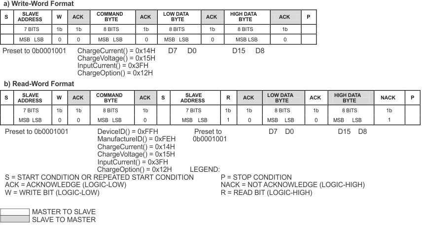
The BQ24725A operates as a slave, receiving control inputs from the embedded controller host through the SMBus interface. The BQ24725A uses a simplified subset of the commands documented in System Management Bus Specification V1.1, which can be downloaded from www.smbus.org. The BQ24725A uses the SMBus Read-Word and Write-Word protocols (see Figure 11) to communicate with the smart battery. The BQ24725A performs only as a SMBus slave device with address 0b00010010 (0x12H) and does not initiate communication on the bus. In addition, the BQ24725A has two identification registers a 16-bit device ID register (0xFFH) and a 16-bit manufacturer ID register (0xFEH).
SMBus communication is enabled with the following conditions:
- VVCC is above UVLO;
- VACDET is above 0.6V;
The data (SDA) and clock (SCL) pins have Schmitt-trigger inputs that can accommodate slow edges. Choose pull-up resistors (10kΩ) for SDA and SCL to achieve rise times according to the SMBus specifications. Communication starts when the master signals a START condition, which is a high-to-low transition on SDA, while SCL is high. When the master has finished communicating, the master issues a STOP condition, which is a low-to-high transition on SDA, while SCL is high. The bus is then free for another transmission. Figure 12 and Figure 13 show the timing diagram for signals on the SMBus interface. The address byte, command byte, and data bytes are transmitted between the START and STOP conditions. The SDA state changes only while SCL is low, except for the START and STOP conditions. Data is transmitted in 8-bit bytes and is sampled on the rising edge of SCL. Nine clock cycles are required to transfer each byte in or out of the BQ24725A because either the master or the slave acknowledges the receipt of the correct byte during the ninth clock cycle. The BQ24725A supports the charger commands as described in Table 2.
 Figure 11. SMBus Write-Word and Read-Word Protocols
  Figure 12. SMBus Write Timing
  Figure 13. SMBus Read Timing