ZHCS229C September 2011 – January 2020 BQ24725A
PRODUCTION DATA.
- 1 特性
- 2 应用
- 3 说明
- 4 修订历史记录
- 5 Pin Configuration and Functions
- 6 Specifications
- 7 Parameter Measurement Information
-
8 Detailed Description
- 8.1 Overview
- 8.2 Functional Block Diagram
- 8.3 Feature Description
- 8.4
Device Functional Modes
- 8.4.1 Adapter Detect and ACOK Output
- 8.4.2 Adapter Over Voltage (ACOVP)
- 8.4.3 System Power Selection
- 8.4.4 Battery LEARN Cycle
- 8.4.5 Enable and Disable Charging
- 8.4.6 Automatic Internal Soft-Start Charger Current
- 8.4.7 High Accuracy Current Sense Amplifier
- 8.4.8 Charge Timeout
- 8.4.9 Converter Operation
- 8.4.10 Continuous Conduction Mode (CCM)
- 8.4.11 Discontinuous Conduction Mode (DCM)
- 8.4.12 Input Over Current Protection (ACOC)
- 8.4.13 Charge Over Current Protection (CHGOCP)
- 8.4.14 Battery Over Voltage Protection (BATOVP)
- 8.4.15 Battery Shorted to Ground (BATLOWV)
- 8.4.16 Thermal Shutdown Protection (TSHUT)
- 8.4.17 EMI Switching Frequency Adjust
- 8.4.18 Inductor Short, MOSFET Short Protection
- 8.5 Register Maps
-
9 Application and Implementation
- 9.1 Application Information
- 9.2
Typical Applications
- 9.2.1
Typical System with Two NMOS Selector
- 9.2.1.1 Design Requirements
- 9.2.1.2
Detailed Design Procedure
- 9.2.1.2.1 Negative Output Voltage Protection
- 9.2.1.2.2 Reverse Input Voltage Protection
- 9.2.1.2.3 Reduce Battery Quiescent Current
- 9.2.1.2.4 Inductor Selection
- 9.2.1.2.5 Input Capacitor
- 9.2.1.2.6 Output Capacitor
- 9.2.1.2.7 Power MOSFETs Selection
- 9.2.1.2.8 Input Filter Design
- 9.2.1.2.9 BQ24725A Design Guideline
- 9.2.1.3 Application Curves
- 9.2.2 Simplified System without Power Path
- 9.2.1
Typical System with Two NMOS Selector
- 9.3 System Examples
- 10Power Supply Recommendations
- 11Layout
- 12器件和文档支持
- 13机械、封装和可订购信息
9.2.1.2.9 BQ24725A Design Guideline
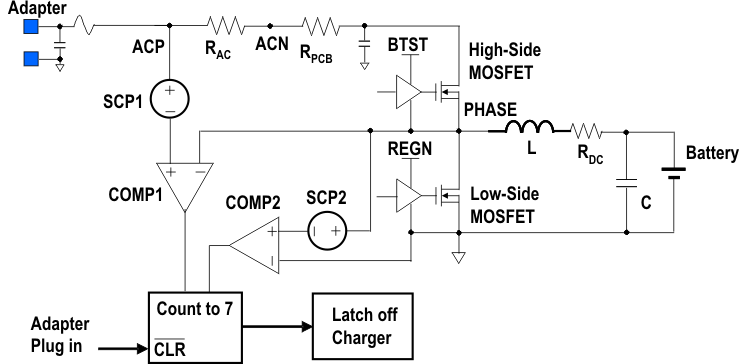
The BQ24725A has a unique short circuit protection feature. Its cycle-by-cycle current monitoring feature is achieved through monitoring the voltage drop across RDS(on) of the MOSFETs after a certain amount of blanking time. For a MOSFET short or inductor short circuit, the over current condition is sensed by two comparators, and two counters are triggered. After seven occurrences of a short circuit event, the charger will be latched off. To reset the charger from latch-off status, reconnect the adapter. Figure 20 shows the BQ24725A short circuit protection block diagram.
 Figure 20. Block Diagram of BQ24725A Short Circuit Protection
 In normal operation, the low side MOSFET current is from source to drain which generates a negative voltage drop when it turns on, as a result the over current comparator can not be triggered. When the high side switch short circuit or inductor short circuit happens, the large current of low side MOSFET is from drain to source and can trig low side switch over current comparator. BQ24725A senses the low side switch voltage drop through the PHASE pin and GND pin.
The high-side FET short is detected by monitoring the voltage drop between ACP and PHASE. As a result, it not only monitors the high side switch voltage drop, but also the adapter sensing resistor voltage drop and PCB trace voltage drop from ACN terminal of RAC to charger high side switch drain. Usually, there is a long trance between input sensing resistor and charger converting input, a careful layout will minimize the trace effect.
To prevent unintentional charger shut down in normal operation, MOSFET RDS(on) selection and PCB layout is very important. Figure 21 shows a improvement PCB layout example and its equivalent circuit. In this layout, the system current path and charger input current path is not separated, as a result, the system current causes voltage drop in the PCB copper and is sensed by the IC. The worst layout is when a system current pull point is after charger input; as a result all system current voltage drops are counted into over current protection comparator. The worst case for IC is when the total system current and charger input current sum equals the DPM current. When the system pulls more current, the charger IC tries to regulate the RAC current as a constant current by reducing the charging current.
 Figure 21. Need improve PCB layout example.
 Figure 22 shows the optimized PCB layout example. The system current path and charge input current path is separated, as a result the IC only senses charger input current caused PCB voltage drop and minimized the possibility of unintentional charger shut down in normal operation. This also makes PCB layout easier for high system current application.
 Figure 22. Optimized PCB layout example.
 The total voltage drop sensed by IC can be express as the following equation.
where the RAC is the AC adapter current sensing resistance, IDPM is the DPM current set point, RPCB is the PCB trace equivalent resistance, ICHRGIN is the charger input current, k is the PCB factor, RDS(on) is the high side MOSFET turn on resistance and IPEAK is the peak current of inductor. Here the PCB factor k equals 0 means the best layout shown in Figure 22 where the PCB trace only goes through charger input current while k equals 1 means the worst layout shown in Figure 21 where the PCB trace goes through all the DPM current. The total voltage drop must below the high side short circuit protection threshold to prevent unintentional charger shut down in normal operation.
The low side MOSFET short circuit voltage drop threshold can be adjusted via SMBus command. ChargeOption() bit[7] =0, 1 set the low side threshold 135mV and 230mV respectively. The high side MOSFET short circuit voltage drop threshold can be adjusted via SMBus command. ChargeOption() bit[8] = 0, 1 disable the function and set the threshold 750mV respectively. For a fixed PCB layout, host should set proper short circuit protection threshold level to prevent unintentional charger shut down in normal operation.