ZHCSG48C April   2015  – March 2017

PRODUCTION DATA.  

  1. 特性
  2. 应用
  3. 说明
  4. 修订历史记录
  5. Pin Configuration and Functions
  6. Specifications
    1. 6.1 Absolute Maximum Ratings
    2. 6.2 ESD Ratings
    3. 6.3 Recommended Operating Conditions
    4. 6.4 Thermal Information
    5. 6.5 Electrical Characteristics
    6. 6.6 Timing Requirements
    7. 6.7 Typical Characteristics
  7. Detailed Description
    1. 7.1 Overview
    2. 7.2 Functional Block Diagram
    3. 7.3 Feature Description
      1. 7.3.1 Device Power Up
        1. 7.3.1.1 Battery Only
        2. 7.3.1.2 Adapter Detect and ACOK Output
          1. 7.3.1.2.1 Adapter Overvoltage (ACOVP)
      2. 7.3.2 System Power Selection
      3. 7.3.3 Enable and Disable Charging
        1. 7.3.3.1 Automatic Internal Soft-Start Charger Current
      4. 7.3.4 Current and Power Monitor
        1. 7.3.4.1 High Accuracy Current Sense Amplifier (IADP and IDCHG)
        2. 7.3.4.2 High Accuracy Power Sense Amplifier (PMON)
      5. 7.3.5 Processor Hot Indication for CPU Throttling
      6. 7.3.6 Converter Operation
        1. 7.3.6.1 Continuous Conduction Mode (CCM)
        2. 7.3.6.2 Discontinuous Conduction Mode (DCM)
        3. 7.3.6.3 Non-Sync Mode and Light Load Comparator
        4. 7.3.6.4 EMI Switching Frequency Adjust
      7. 7.3.7 Battery LEARN Cycle
      8. 7.3.8 Charger Timeout
      9. 7.3.9 Device Protections Features
        1. 7.3.9.1 Input Overcurrent Protection (ACOC)
        2. 7.3.9.2 Charge Overcurrent Protection (CHGOCP)
        3. 7.3.9.3 Battery Overvoltage Protection (BATOVP)
        4. 7.3.9.4 Battery Short
        5. 7.3.9.5 Thermal Shutdown Protection (TSHUT)
        6. 7.3.9.6 Inductor Short, MOSFET Short Protection
    4. 7.4 Device Functional Modes
      1. 7.4.1 Battery Charging
      2. 7.4.2 Hybrid Power Boost Mode
        1. 7.4.2.1 Battery Discharge Current Regulation in Hybrid Power Boost Mode
    5. 7.5 Programming
      1. 7.5.1 SMBus Interface
        1. 7.5.1.1 SMBus Write-Word and Read-Word Protocols
        2. 7.5.1.2 Timing Diagrams
    6. 7.6 Register Maps
      1. 7.6.1  Battery-Charger Commands
      2. 7.6.2  Setting Charger Options
        1. 7.6.2.1 ChargeOption0 Register
      3. 7.6.3  ChargeOption1 Register
      4. 7.6.4  ChargeOption2 Register
      5. 7.6.5  ChargeOption3 Register
      6. 7.6.6  ProchotOption0 Register
      7. 7.6.7  ProchotOption1 Register
      8. 7.6.8  ProchotStatus Register
      9. 7.6.9  Setting the Charge Current
      10. 7.6.10 Setting the Charge Voltage
      11. 7.6.11 Setting Input Current
      12. 7.6.12 Setting the Discharge Current
  8. Application and Implementation
    1. 8.1 Application Information
    2. 8.2 Typical Applications
      1. 8.2.1 Design Requirements
      2. 8.2.2 Detailed Design Procedure
        1. 8.2.2.1 Negative Output Voltage Protection
        2. 8.2.2.2 Reverse Input Voltage Protection
        3. 8.2.2.3 Reduce Battery Quiescent Current
        4. 8.2.2.4 Inductor Selection
        5. 8.2.2.5 Input Capacitor
        6. 8.2.2.6 Output Capacitor
        7. 8.2.2.7 Power MOSFETs Selection
        8. 8.2.2.8 Input Filter Design
      3. 8.2.3 Application Curves
  9. Power Supply Recommendations
  10. 10Layout
    1. 10.1 Layout Guidelines
    2. 10.2 Layout Examples
      1. 10.2.1 Layout Consideration of Current Path
      2. 10.2.2 Layout Consideration of Short Circuit Protection
      3. 10.2.3 Layout Consideration for Short Circuit Protection
  11. 11器件和文档支持
    1. 11.1 接收文档更新通知
    2. 11.2 社区资源
    3. 11.3 商标
    4. 11.4 静电放电警告
    5. 11.5 Glossary
  12. 12机械、封装和可订购信息

封装选项

机械数据 (封装 | 引脚)
散热焊盘机械数据 (封装 | 引脚)
订购信息

Specifications

Absolute Maximum Ratings

over operating free-air temperature range (unless otherwise noted)(1)(2)
MIN MAX UNIT
Voltage SRN, SRP, ACN, ACP, CMSRC, VCC, BATSRC –0.3 30 V
PHASE –2 30
ACDET, SDA, SCL, LODRV, REGN, IADP, IDCHG, PMON, ILIM, ACOK, CMPIN, CMPOUT, BATPRES, TB_STAT –0.3 7
PROCHOT –0.3 5.7
BTST, HIDRV, ACDRV, BATDRV –0.3 36
Differential voltage BTST-PHASE, HIDRV-PHASE ACDRV-CMSRC, BATDRV-BATSRC –0.3 7 V
Voltage LODRV (2% duty cycle) –4 7 V
HIDRV (2% duty cycle) –4 36
Voltage PHASE (2% duty cycle) –4 30 V
Voltage REGN (5ms) –0.3 9 V
Maximum differential voltage SRP–SRN, ACP–ACN –0.5 +0.5 V
Junction temperature, TJ –40 155 °C
Storage temperature, Tstg –55 155 °C
Stresses beyond those listed under absolute maximum ratings may cause permanent damage to the device. These are stress ratings only, and functional operation of the device at these or any other conditions beyond those indicated under recommended operating conditions is not implied. Exposure to absolute-maximum-rated conditions for extended periods may affect device reliability.
All voltages are with respect to GND if not specified. Currents are positive into, negative out of the specified pin. Consult Packaging Section of the data book for thermal limitations and considerations of packages.

ESD Ratings

VALUE UNIT
V(ESD) Electrostatic discharge Human body model (HBM), per ANSI/ESDA/JEDEC JS-001 (1) ±2000 V
Charged device model (CDM), per JEDEC specification JESD22-C101 (2) ±500
JEDEC document JEP155 states that 500-V HBM allows safe manufacturing with a standard ESD control process.
JEDEC document JEP157 states that 250-V CDM allows safe manufacturing with a standard ESD control process.

Recommended Operating Conditions

over operating free-air temperature range (unless otherwise noted)
MIN MAX UNIT
Voltage SRN, SRP, ACN, ACP, CMSRC, VCC, BATSRC 0 24 V
PHASE –2 24
ACDET, SDA, SCL, LODRV, REGN, IADP, IDCHG, PMON, ILIM, ACOK, CMPIN, CMPOUT, BATPRES, TB_STAT 0 6.5
PROCHOT –0.3 5
BTST, HIDRV, ACDRV, BATDRV 0 30
Maximum difference SRP–SRN, ACP–ACN –0.4 +0.4 V
Junction temperature, TJ –20 125 °C
Operating free-air temperature, TA –40 85

Thermal Information

THERMAL METRIC(1) bq24780S UNIT
RUY (WQFN)
28 PINS
RθJA Junction-to-ambient thermal resistance 33.3 °C/W
RθJCtop Junction-to-case (top) thermal resistance 29.7 °C/W
RθJB Junction-to-board thermal resistance 6.5 °C/W
ψJT Junction-to-top characterization parameter 0.3 °C/W
ψJB Junction-to-board characterization parameter 6.5 °C/W
RθJCbot Junction-to-case (bottom) thermal resistance 1.3 °C/W
For more information about traditional and new thermal metrics, see the IC Package Thermal Metrics application report, SPRA953.

Electrical Characteristics

4.5 V ≤ VVCC ≤ 24 V, –40°C ≤ TJ ≤ 125°C, typical values are at TA = 25°C, with respect to GND (unless otherwise noted)
PARAMETER TEST CONDITIONS MIN TYP MAX UNIT
OPERATING CONDITIONS
VVCC(OP) VCC/ACP/ACN operating voltage 4.5 24 V
CHARGE VOLTAGE REGULATION
VBAT(REG_RNG) Battery voltage 1.024 19.2 V
VBAT(REG_ACC) Charge voltage regulation accuracy ChargeVoltage() = 0x41A0 16.8 V
–10°C-85°C –0.4% 0.4%
–40°C-125°C –0.5% 0.5%
ChargeVoltage() = 0x3130 12.592 V
–10°C-85°C –0.4% 0.4%
–40°C-125°C –0.5% 0.5%
ChargeVoltage() = 0x20D0 8.4 V
–10°C-85°C –0.4% 0.4%
–40°C-125°C –0.6% 0.6%
ChargeVoltage() = 0x1060 4.192 V
–10°C-85°C –0.5% 0.8%
–40°C-125°C –0.7% 0.8%
CHARGE CURRENT REGULATION
VIREG(CHG_RNG) Charge current regulation differential voltage VIREG(CHG) = VSRP – VSRN 0 81.28 mV
ICHRG(REG_ACC) Charge current regulation accuracy
(SRN > 2.8 V)
ChargeCurrent() = 0x1000 4096 mA
–2% 2%
ChargeCurrent() = 0x0800 2048 mA
–3% 3%
ChargeCurrent() = 0x0200 512 mA
–10% 10%
ChargeCurrent() = 0x0100 256 mA
ChargeVoltage() = 0x20D0, 0x3031, 0x41A0 –16% 16%
ChargeVoltage() = 0x1060 –20% 20%
ChargeCurrent() = 0x00C0 192 mA
–20% 20%
ChargeCurrent() = 0x0080 128 mA
–30% 30%
ILGK(SRP-SRN) SRP and SRN leakage mismatch –8 8 µA
DISCHARGE CURRENT REGULATION
V(IREG_CHG_RNG) Charge current regulation differential voltage VIREG(IDISCHG) = VSRN – VSRP 0 322.56 mV
I(DCHRG_REG_ACC) Discharge current regulation accuracy ChargeCurrent() = 0x2000 8192 mA
–2% 2%
ChargeCurrent() = 0x1000 4096 mA
–3% 3%
ChargeCurrent() = 0x0800 2048 mA
–5% 5%
ChargeCurrent() = 0x0400 1024 mA
–8% 8%
ChargeCurrent() = 0x0400 512 mA
–10% 10%
INPUT CURRENT REGULATION
V(IREG_DPM_RNG) Input current regulation differential voltage V(IREG_DPM) = V(ACP) – V(ACN) 0 80.64 mV
I(DPM_REG_ACC) Input current regulation accuracy InputCurrent() = 0x1000 4096 mA
–2% 2%
InputCurrent() = 0x0800 2048 mA
–3% 3%
InputCurrent() = 0x0400 1024 mA
–5% 5%
InputCurrent() = 0x0200 512 mA
–12% 12%
ILGK(ACP-ARN) ACP and ACN leakage mismatch –5 5 µA
INPUT CURRENT SENSE AMPLIFIER
V(IADP) IADP output voltage 0 3.3 V
I(IADP) IADPT output current 0 1 mA
A(IADP) IADP sense amplifier gain V(IADP) / V(ACP-ACN), REG0x12[4] = 0 20 V/V
V(IADP_ACC) Current sense amplifier gain accuracy V(ACP-ACN) = 40 mV –2% 2%
V(ACP-ACN) = 20 mV –4% 4%
V(ACP-ACN) ≥ 10 mV –7% 7%
V(ACP-ACN) ≥ 5 mV –20% 20%
V(ACP-ACN) ≥ 2.5 mV –30% 30%
V(ACP-ACN) ≥ 1.5 mV –40% 40%
V(IADP_CLAMP) IADP clamp voltage 3 3.3 V
C(IADP) IADP output load capacitance With 0 to 1mA load 100 pF
DISCHARGE CURRENT SENSE AMPLIFIER
V(IDCHG) IDCHG output voltage 0 3.3 V
I(IDCHG) IDCHG output current 0 1 mA
A(IDCHG) Current sense amplifier gain V(IDCHG)/V(SRN-SRP), REG0x12[3] = 1 16 V/V
V(IDCHG_ACC) Current sense output accuracy V(SRN-SRP) = 40 mV –5% 5%
V(SRN-SRP) = 20 mV –9% 9%
V(SRN-SRP) = 10 mV –17% 17%
V(SRN-SRP) = 5 mV –34% 34%
V(IDCHG_CLAMP) IDCHG clamp voltage 3 3.3 V
C(IDCHG) IDCHG output load capacitance With 0 to 1mA load 100 pF
SYSTEM POWER SENSE AMPLIFIER
V(PMON) PMON output voltage 0 3.3 V
I(PMON) PMON output current 0 160 µA
A(PMON) PMON system gain V(PMON)/(PIN + PBAT, REG0x3B[9] = 1 1 µA/W
VPMON_ACC PMON Gain Accuracy
(REG0x3B[9]=1)
Adapter Only with System Power = 19.5V/45W –4% 4%
Adapter Only with System Power = 12V/24W –6% 6%
Adapter Only with System Power = 5V/9W –10% 10%
Battery Only with System Power 11V/44W –4.5% 4.5%
Battery Only with System Power 7.4V/29.8W –7% 7%
Battery Only with System Power 3.7V/14.4W –10% 10%
VPMON_CLAMP PMON clamp voltage 3% 3.3% V
CPMON Maximum output load capacitance With 0 to 1 mA 100 pF
REGN REGULATOR
V(REGN_REG) REGN regulator voltage VVCC > V(UVLO), V(ACDET) > V(wakeup_RISE) 5.7 6 6.3 V
I(REGN_LIM_Charging) REGN current limit when in charging mode V(REGN) = 0 V, VVCC > V(UVLO), in charging mode 80 100 mA
VLDO(DROPOUT) REGN output voltage in dropout VVCC = 5 V, ILOAD = 20 mA 4.4 4.6 4.75 V
I(REGN_LIM) REGN current limit when not in charging VREGN = 0 V, VVCC > V(UVLO), Not in charging mode 13 mA
I(REGN_TSHUT) REGN output under thermal shutdown VREGN = 5V 13 23 mA
C(REGN) REGN output capacitor ILOAD = 100 µA to 50 mA 2.2 μF
VCC UNDER VOLTAGE LOCKOUT COMPARATOR
VVCC(UVLO) Input undervoltage rising threshold VCC rising 2.4 2.6 2.8 V
VVCC(UVLO_HYS) Input undervoltage falling hysteresis 200 mV
QUIESCENT CURRENT
IBAT Current with battery only,
TJ = 0 to 85°C,
ISRN + ISRP + IBATSRC + IPHASE + IVCC + IACP + IACN
VBAT = 16.8 V, VCC disconnected from battery, REG0x12[15] = 1 5 μA
VBAT = 16.8 V, VCC connected from battery, REG0x12[15] = 1 25 44
VBAT = 16.8 V, VCC connect to battery, BATFET on, REG0x12[15] = 0, REGN = 0 V, Comparator and PROCHOT enabled, PMON disabled, TJ = 0 to 85°C 700 800
IAC Adapter current,
IVCC + IACP + IACN + IACDRV + ICMSRC
V(VCC_ULVO) < VVCC < V(ACOVP), V(ACDET) > 2.4 V, charge disabled 0.65 0.8 mA
V(VCC_ULVO) < VVCC < V(ACOVP), V(ACDET) > 2.4 V, charge enabled, no switching 1.6 3
V(VCC_ULVO) < VVCC < V(ACOVP), V(ACDET) > 2.4 V, charge enabled, switching, MOSFET Qg 4nC 10
ACOK COMPARATOR
V(ACOK_RISE) ACOK rising threshold VVCC > V(VCC_UVLO), ACDET ramps up 2.375 2.4 2.425 V
V(ACOK_FALL) ACOK falling threshold VVCC > V(VCC_UVLO), ACDET ramps down 2.3 2.345 2.395 V
V(WAKEUP_RISE) WAKEUP detect rising threshold VVCC > V(VCC_UVLO), ACDET ramps up 0.57 0.8 V
V(WAKEUP_FALL) WAKEUP detect falling threshold VVCC > V(VCC_UVLO), ACDET ramps down 0.3 0.51 V
VCC to SRN COMPARATOR (VCC_SRN)
V(VCC-SRN_FALL) VCC-SRN falling threshold to turn off ACFET VCC ramps down to SRN –20 60 140 mV
V(VCC-SRN _RISE) VCC-SRN rising threshold to turn on ACFET VCC ramps up above SRN 170 260 360 mV
ACN to SRN COMPARATOR (ACN_SRN)
V(ACN-SRN_FALL) ACN to BAT falling threshold VCC ramps up above SRN ACN ramps down towards SRN 120 200 280 mV
V(ACN- SRN _RISE) ACN to BAT rising threshold to turn on BATFET ACN ramps above SRN 220 290 360 mV
HIGH SIDE IFAULT COMPARATOR (IFAULT_HI)
V(ACN_PH_RISE) ACN to PH rising threshold reg0x37 bit [7] = 0 450 750 1200 mV
LOW SIDE IFAULT COMPARATOR (IFAULT_LOW)
V(IFAULT_LO_RISE) PHASE to GND rising threshold reg0x37 bit [6] = 1 180 250 340 mV
INPUT OVERVOLTAGE COMPARATOR (ACOVP)
V(ACOV) VCC overvoltage rising threshold VCC ramps up 24 26 28 V
V(ACOV_HYS) VCC overvoltage falling hysteresis VCC ramps down 1 V
INPUT OVERCURRENT COMPARATOR (ACOC)
V(ACOC) Rising threshold w.r.t. ICRIT input current limit REG0x37[9] = 1 180% 200% 220%
V(ACOC_CLAMP) ACOC threshold V(ACP) – V(ACN) 50 190 mV
BAT OVERVOLTAGE COMPARATOR (BAT_OVP)
VOVP(RISE) Overvoltage rising threshold as percentage of VBAT(REG) SRN ramps up 103% 104% 106%
VOVP(FALL) Overvoltage falling threshold as percentage of VBAT(REG) SRN ramps down 102%
IOVP Discharge resistor on SRP VSRN > 6 V 6 mA
VSRN = 4.5 V 2.5
CHARGE OVERCURRENT COMPARATOR (CHG_OCP)
VOCP(limit) Cycle-by-cycle overcurrent limit, measured voltage between SRP and SRN ChargeCurrent() = 0x0xxxH 54 60 66 mV
ChargeCurrent() = 0x1000H – 0x17C0H 80 90 100 mV
ChargeCurrent() = 0x1800H – 0x1FC0H 110 120 130 mV
CHARGE UNDERCURRENT COMPARATOR (CHG_UCP)
VUCP(FALL) Cycle-by-cycle undercurrent falling threshold SRP ramps down towards SRN 1 5 9 mV
LIGHT LOAD COMPARATOR (LIGHT_LOAD)
VLL(FALL) Light load falling threshold SRP ramps down towards SRN 1.25 mV
VLL(RISE_HYST) Light load rising hysteresis SRP ramps above SRN 1.25 mV
BATTERY DEPLETION COMPARATOR (BAT_DEPL)
VBAT(DEPL_FALL) Battery depletion falling threshold, as percentage of voltage regulation limit REG0x3B[15:14] = 00 56% 60% 64%
REG0x3B[15:14] = 01 60% 64% 68%
REG0x3B[15:14] = 10 64% 68% 72%
REG0x3B[15:14] = 11 68% 72% 78%
VBAT(DEPL_RISE_ HYST) Battery depletion rising hysteresis REG0x3B[15:14] = 00 225 305 400 mV
REG0x3B[15:14] = 01 240 325 430
REG0x3B[15:14] = 10 255 345 450
REG0x3B[15:14] = 11 280 370 490
VBAT(DEPL_RDEG) Battery depletion rising deglitch Delay to turn on BATFET and turn off ACFET during LEARN cycle 600 ms
VBAT(DEPL_FDEG) Battery depletion falling deglitch Delay to turn off BATFET and turn on ACFET during LEARN cycle 10 µs
BATTERY LOWV COMPARATOR (BAT_LOWV)
VBAT(LV_FALL) Battery LOWV falling threshold SRN ramps down 2.3 2.5 2.8 V
VBAT(LV_RHYST) Battery LOWV rising hysteresis SRN ramps up 200 mV
IBAT(LV_RESET) Battery LOWV charge current limit Measure across SRP and SRN 5 mV
THERMAL SHUTDOWN COMPARATOR (TSHUT)
TSHUT Thermal shutdown rising temperature Temperature ramps up 155 °C
TSHUT(HYS) Thermal shutdown hysteresis, falling Temperature ramps down 20 °C
ILIM COMPARATOR
VILIM(FALL) ILIM as converter enable falling threshold VILIM falling 60 75 90 mV
VILIM(RISE) ILIM as converter enable rising threshold VILIM rising 90 105 120 mV
INDEPENDENT COMPARATOR
V(CMPOS) Comparator input offset –4 4 mV
V(CMPCM) Comparator input common-mode 0 6.5 V
V(CMPREF) Comparator reference voltage (CMPIN falling) REG0x3B[7] = 0 2.28 2.3 2.32 V
REG0x3B[7] = 1 1.18 1.2 1.22 V
V(CMPRISE) Comparator reference hysteresis REG0x3B[6] = 0 100 mV
PWM OSCILLATOR
FSW PWM switching frequency REG0x12[9:8] = 00 510 600 690 kHz
REG0x12[9:8] = 01 680 800 920
REG0x12[9:8] = 10 850 1000 1150
BATFET GATE DRIVER (BATDRV)
IBAT(FET) BATDRV charge pump current limit VBAT(DRV) – VBAT(SRC) = 5 V 40 60 µA
Gate drive voltage on BATFET VBAT(DRV) – VBAT(SRC) when V(SRN) > VBAT(UVLO) 5.5 6.1 6.8 V
RBAT(DRV_OFF) BATDRV turn-off resistance 5 6.2 7.4
RBAT(DRV_LOAD) Minimum Load between gate and source 500
ACFET GATE DRIVER (ACDRV)
I(ACFET) ACDRV charge pump current limit V(ACDRV) – V(CMSRC) = 5 V 40 60 µA
Gate drive voltage on ACFET V(ACDRV) – V(CMSRC) when VVCC > V(UVLO) 5.5 6.1 6.8 V
R(ACDRV_OFF) ACDRV turn-off resistance 5 6.2 7.4
R(ACDRV_LOAD) Minimum load between gate and source 500
PWM HIGH SIDE DRIVER (HIDRV)
RDS(HI_ON) High-side driver (HSD) turn-on resistance V(BTST) – V(PH) = 5.5 V 6 10 Ω
RDS(HI_OFF) High-side driver (HSD) turn-off Resistance V(BTST) – V(PH) = 5.5 V 0.9 1.4 Ω
V(BTST_REFRESH) Bootstrap refresh comparator threshold voltage V(BTST) – V(PH) when low side refresh pulse is requested 3.85 4.3 4.7 V
PWM LOW SIDE DRIVER (LODRV)
RDS(LO_ON) Low-side driver (LSD) turn-on resistance 7.5 12 Ω
RDS(LO_OFF) Low-side driver (LSD) turn-off resistance 0.75 1.25 Ω
INTERNAL SOFT START
ISTEP Soft start step size 64 mA
tSTEP Soft start step time 400 µs
PROCHOT
V(ICRIT) ICRIT comparator threshold REG0x3C[15:11] = 01001, as percentage of input current limit, InputCurrent() = 0x1000 147% 150% 153%
V(INOM) INOM comparator threshold as percentage of input current limit, InputCurrent()=0x0800 107% 110% 112%
V(IDCHG) IDCHG comparator threshold REG0x3D[15:11] = 10000, as voltage between SRN and SRP 160 163.84 167 mV
REG0x3D[15:11] = 00100, as voltage between SRN and SRP 38 40.96 44
V(VSYS) VSYS comparator threshold REG0x3C[7:6] = 01 5.88 6 6.12 V
LOGIC INPUT (SDA, SCL, BATPRES)
VIN(LO) Input low threshold 0.8 V
VIN(HI) Input high threshold 2.1 V
VIN(LEAK) Input bias current V = 7 V –1 µA
LOGIC OUTPUT OPEN DRAIN (ACOK, SDA, CMPOUT, TB_STAT)
VO(LO) Output saturation voltage 5-mA drain current 500 mV
VO(LEAK) Leakage current V = 7 V –1 1 µA
LOGIC OUTPUT OPEN DRAIN (PROCHOT)
VO(LEAK_PROCHOT) Output saturation voltage 17-mA drain current 300 mV
Leakage current V = 5.5 V –1 1 µA

Timing Requirements

4.5 V ≤ VVCC ≤ 24 V, –40°C ≤ TJ ≤ 125°C, typical values are at TA = 25°C, with respect to GND (unless otherwise noted)
PARAMETER MIN TYP MAX UNIT
ACOK COMPARATOR
tACOK_RISE_DEG ACOK rising deglitch to turn on
ACFET; VACDET > 2.4V [GBD]
VVCC > VVCC_UVLO, ACDET ramps up,
1st time or REG0x12[12] = 0
100 150 200 ms
VVCC > VVCC_UVLO, ACDET ramps up,
Not 1st time or REG0x12[12] = 1
0.9 1.3 1.7 s
tACOK_FALL_DEG ACOK falling deglitch to turn off
ACFET [GBD]
VVCC > VVCC_UVLO, ACDET ramps down 3 µs
INPUT OVERCURRENT COMPARATOR (ACOC)
tACOC_DEG Deglitch time to latch off ACFET 9 12 15 ms
SMBus TIMING CHARACTERISTICS
tR SCLK/SDATA rise time 1 µs
tF SCLK/SDATA fall time 300 ns
tW(H) SCLK pulse width high 4 50 µs
tW(L) SCLK pulse width low 4.7 µs
tSU(STA) Setup time for start condition 4.7 µs
tH(STA) Start condition hold time after which first clock pulse is generated 4 µs
tSU(DAT) Data setup time 250 ns
tH(DAT) Data hold time 300 ns
tSU(STOP) Setup time for stop condition 4 µs
t(BUF) Bus free time between start and stop condition 4.7 µs
FS(CL) Clock frequency 10 100 kHz
HOST COMMUNICATION FAILURE
ttimeout SMBus bus release timeout(1) 25 35 ms
tBOOT Deglitch for watchdog reset signal 10 ms
tWDI Watchdog timeout period, REG0x12 [14:13] = 01(2) 4 5 6 s
tWDI Watchdog timeout period, REG0x12 [14:13] = 10(2) 70 88 105
tWDI Watchdog timeout period, REG0x12 [14:13] = 11(2) (default) 140 175 210
PWM DRIVER TIMING
tDEADTIME_RISE Driver dead time from low side to high side 20 ns
tDEADTIME_FALL Driver dead time from high side to low side 20 ns
Devices participating in a transfer timeout when any clock low exceeds the 25-ms minimum timeout period. Devices that have detected a timeout condition must reset the communication no later than the 35-ms maximum timeout period. Both a master and a slave must adhere to the maximum value specified because it incorporates the cumulative stretch limit for both a master (10 ms) and a slave (25 ms).
User can adjust threshold through SMBus ChargeOption() REG0x12.
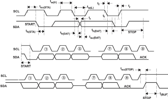
bq24780S timing_SMBus_SLUSBW0.gif Figure 1. SMBus Communication Timing Waveforms

Typical Characteristics

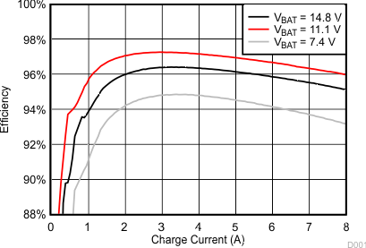
bq24780S G200_slusc27.gif
VIN = 20 V
Figure 2. Efficiency During Charging
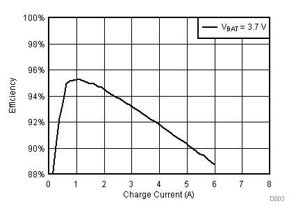
bq24780S D003_SLUSC27.gif
VIN = 5 V
Figure 4. Efficiency During Charging
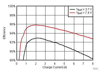
bq24780S D002_SLUSC27.gif
VIN = 12 V
Figure 3. Efficiency During Charging
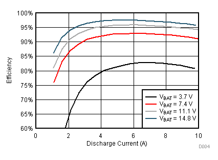
bq24780S D004_SLUSC27.gif
VIN = 20 V
Figure 5. Efficiency During Boost