ZHCSDZ5C August 2014 – November 2014
UNLESS OTHERWISE NOTED, this document contains PRODUCTION DATA.
- 1 特性
- 2 应用
- 3 说明
- 4 修订历史记录
- 5 Device Comparison Table
- 6 Pin Configuration and Functions
- 7 Specifications
-
8 Detailed Description
- 8.1 Overview
- 8.2 Functional Block Diagram
- 8.3
Feature Description
- 8.3.1 Overvoltage-Protection (OVP) - Continuously Monitored
- 8.3.2 CHG Pin Indication (bq25101, bq25101H)
- 8.3.3 CHG Pin LED Pull-up Source (bq25101, bq25101H)
- 8.3.4 IN-DPM (VIN-DPM or IN-DPM)
- 8.3.5 OUT
- 8.3.6 ISET
- 8.3.7 PRE_TERM - Pre-Charge and Termination Programmable Threshold
- 8.3.8 TS
- 8.3.9 Timers
- 8.3.10 Termination
- 8.4 Device Functional Modes
- 9 Application and Implementation
- 10Power Supply Recommendations
- 11Layout
- 12器件和文档支持
- 13机械、封装和可订购信息
9 Application and Implementation
NOTE
Information in the following applications sections is not part of the TI component specification, and TI does not warrant its accuracy or completeness. TI’s customers are responsible for determining suitability of components for their purposes. Customers should validate and test their design implementation to confirm system functionality.
9.1 Application Information
The bq2510x series of devices are highly integrated Li-Ion and Li-Pol linear chargers targeted at space-limited portable applications. The fast charge current can be programmed from 10 mA to 250 mA through an external resistor on ISET pin. The pre_charge and termination current can also be programmed through the resistor connected on PRETERM pin. The device has complete system-level protection such as input under-voltage lockout (UVLO), input over-voltage protection (OVP), sleep mode, thermal regulation, safety timers, and NTC monitoring input.
9.2 Typical Application - Charger Application Design Example
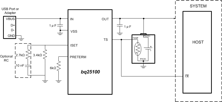
9.2.1 Design Requirements
- Supply voltage = 5 V
- Fast charge current: IOUT-FC = 40 mA;
- Termination Current Threshold: %IOUT-FC = 10% of Fast Charge or ~4 mA
- Pre-Charge Current by default is twice the termination Current or ~8 mA
- TS – Battery Temperature Sense = 10-k NTC (103AT)
- /CE is an open drain control pin
9.2.2 Detailed Design Procedures
- The regulation voltage is set to 4.2 V, the input voltage is 5 V and the charge current is programmed to 40 mA.
- For charge current that is below 50 mA, an extra RC circuit is recommended on ISET to acheive more stable current signal. For applications that need higher charge current, the RC circuit is not needed.
- For applications that use more than 200-mA current, there could be a very low level ~1% of charge current ringing in the output. The ringing can be removed by increasing the input capacitance.
9.2.2.1 Calculations
9.2.2.1.1 Program the Fast Charge Current, ISET:
RISET = [K(ISET) / I(OUT)]
from electrical characteristics table. . . K(SET) = 135 AΩ
RISET = [135 AΩ/0.04 A] = 3.4 kΩ
Selecting the closest standard value, use a 3.4-kΩ resistor between ISET and Vss.
9.2.2.1.2 Program the Termination Current Threshold, ITERM:
RPRE-TERM = K(TERM) × %IOUT-FC
RPRE-TERM = 600 Ω/% × 10% = 6 kΩ
Selecting the closest standard value, use a 6-kΩ resistor between PRETERM and Vss.
One can arrive at the same value by using 20% for a pre-charge value (factor of 2 difference).
RPRE-TERM = K(PRE-CHG) × %IOUT-FC
RPRE-TERM = 300 Ω/% × 20%= 6 kΩ
9.2.2.1.3 TS Function
Use a 10-k NTC thermistor in the battery pack (103AT).
To Disable the temp sense function, use a fixed 10-kΩ resistor between the TS and VSS.
9.2.2.1.4 Selecting IN and OUT Pin Capacitors
In most applications, all that is needed is a high-frequency decoupling capacitor (ceramic) on the power pin, input and output pins. Using the values shown on the application diagram is recommended. After evaluation of these voltage signals with real system operational conditions, one can determine if capacitance values can be adjusted toward the minimum recommended values (DC load application) or higher values for fast, high amplitude, pulsed load applications. Note if designed for high input voltage sources (bad adaptors or wrong adaptors), the capacitor needs to be rated appropriately. Ceramic capacitors are tested to 2x their rated values so a 16-V capacitor may be adequate for a 30-V transient (verify tested rating with capacitor manufacturer).
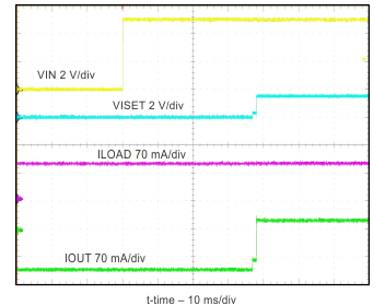
9.2.3 bq25100 Application Performance Plots
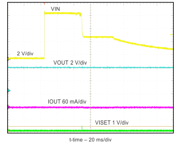
| Hot Plug | ||
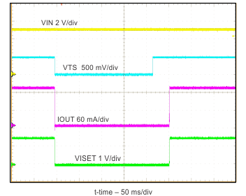
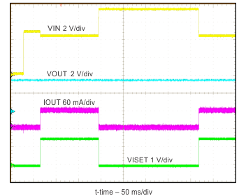
| VIN 0 V -5 V-7 V-5 V | ||
| 90-mA Load, 120-mA IOUT | ||