ZHCSHF5A May 2017 – January 2018
PRODUCTION DATA.
- 1 特性
- 2 应用
- 3 说明
- 4 修订历史记录
- 5 说明 (续)
- 6 Device Comparison Table
- 7 Pin Configuration and Functions
- 8 Specifications
-
9 Detailed Description
- 9.1 Overview
- 9.2 Functional Block Diagram
- 9.3
Feature Description
- 9.3.1 Ship Mode
- 9.3.2 High Impedance Mode
- 9.3.3 Active Battery Only Connected
- 9.3.4 Voltage Based Battery Monitor
- 9.3.5 Sleep Mode
- 9.3.6 Input Voltage Based Dynamic Power Management (VIN(DPM))
- 9.3.7 Input Overvoltage Protection and Undervoltage Status Indication
- 9.3.8 Battery Charging Process and Charge Profile
- 9.3.9 Dynamic Power Path Management Mode
- 9.3.10 Battery Supplement Mode
- 9.3.11 Default Mode
- 9.3.12 Termination and Pre-Charge Current Programming by External Components (IPRETERM)
- 9.3.13 Input Current Limit Programming by External Components (ILIM)
- 9.3.14 Charge Current Programming by External Components (ISET)
- 9.3.15 Safety Timer and Watchdog Timer
- 9.3.16 External NTC Monitoring (TS)
- 9.3.17 Thermal Protection
- 9.3.18 Typical Application Power Dissipation
- 9.3.19 Status Indicators (PG and INT)
- 9.3.20 Chip Disable (CD)
- 9.3.21 Buck (PWM) Output
- 9.3.22 Load Switch / LDO Output and Control
- 9.3.23 Manual Reset Timer and Reset Output (MR and RESET)
- 9.4 Device Functional Modes
- 9.5 Programming
- 9.6
Register Maps
- 9.6.1 Status and Ship Mode Control Register
- 9.6.2 Faults and Faults Mask Register
- 9.6.3 TS Control and Faults Masks Register
- 9.6.4 Fast Charge Control Register
- 9.6.5 Termination/Pre-Charge and I2C Address Register
- 9.6.6 Battery Voltage Control Register
- 9.6.7 SYS VOUT Control Register
- 9.6.8 Load Switch and LDO Control Register
- 9.6.9 Push-button Control Register
- 9.6.10 ILIM and Battery UVLO Control Register
- 9.6.11 Voltage Based Battery Monitor Register
- 9.6.12 VIN_DPM and Timers Register
- 10Application and Implementation
- 11Power Supply Recommendations
- 12Layout
- 13器件和文档支持
- 14机械、封装和可订购信息
9.3.1.1 Ship Mode Entry and Exit
The device may only enter Ship Mode when there is not a valid VIN supply present (VIN< VUVLO). Once the IN supply is removed there are two ways for the device to enter Ship Mode: through I2C command using the EN_SHIPMODE bit and by doing a long button press when MRREC bit is set to 0. If the EN_SHIPMODE bit is set while the IN supply is present, the device will enter Ship Mode upon removal of the supply. The EN_SHIPMODE bit can be cleared using the I2C interface as well while the IN input is valid.
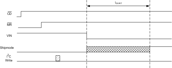
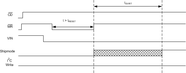
In addition to VIN< VUVLO, CD and MR must be high. Once all of these conditions are met the device will begin the transition to Ship Mode. All three conditions must remain unchanged for a period of tQUIET to ensure proper operation. Figure 15 and Figure 16show the correct sequencing to ensure proper entry into the Ship Mode through I2C command and MR button press respectively.
 Figure 15. CD, MR and VIN Sequencing for Ship Mode Entry Through I2C Command
 Figure 16. CD, MR and VIN Sequencing for Ship Mode Entry Through Long MR button press
The end user can enable the device (exit Ship Mode) by connecting an adapter to IN (VIN> VBAT + VSLP) or by toggling the MR button. Note that in the case where an adapter is connected while the MR is still held low and immediately after the RESET timer has expired (MR low for tRESET), the device will not enter Ship Mode, but may enter it upon adapter removal (Same behavior as setting the EN_SHIPMODE bit when the adapter is present). This will not be the case if MR has gone high when the adapter is connected or MR continues to be held low for a period longer than tWAKE1 after the adapter is connected.
To exit Ship Mode through and MR press the battery voltage must be above the maximum programmable BUVLO threshold when VIN is not present. Once MR goes low, the device will start to exit Ship Mode, powering PMID. The device will not complete the transition from Ship Mode until MR has been held low for at least tWAKE1. Only after the transition is complete may the host start I2C communication if the device has not entered High Impedance Mode.