ZHCSH42A November 2017 – January 2021 BQ25122
PRODUCTION DATA
- 1 特性
- 2 应用
- 3 说明
- 4 Revision History
- 5 说明(续)
- 6 Device Comparison Table
- 7 Pin Configuration and Functions
- 8 Specifications
-
9 Detailed Description
- 9.1 Overview
- 9.2 Functional Block Diagram
- 9.3
Feature Description
- 9.3.1 Ship Mode
- 9.3.2 High Impedance Mode
- 9.3.3 Active Battery Only Connected
- 9.3.4 Voltage Based Battery Monitor
- 9.3.5 Sleep Mode
- 9.3.6 Input Voltage Based Dynamic Power Management (VIN(DPM))
- 9.3.7 Input Overvoltage Protection and Undervoltage Status Indication
- 9.3.8 Battery Charging Process and Charge Profile
- 9.3.9 Dynamic Power Path Management Mode
- 9.3.10 Battery Supplement Mode
- 9.3.11 Default Mode
- 9.3.12 Termination and Pre-Charge Current Programming by External Components (IPRETERM)
- 9.3.13 Input Current Limit Programming by External Components (ILIM)
- 9.3.14 Charge Current Programming by External Components (ISET)
- 9.3.15 Safety Timer and Watchdog Timer
- 9.3.16 External NTC Monitoring (TS)
- 9.3.17 Thermal Protection
- 9.3.18 Typical Application Power Dissipation
- 9.3.19 Status Indicators ( PG and INT)
- 9.3.20 Chip Disable ( CD)
- 9.3.21 Buck (PWM) Output
- 9.3.22 Load Switch / LDO Output and Control
- 9.3.23 Manual Reset Timer and Reset Output ( MR and RESET)
- 9.4 Device Functional Modes
- 9.5 Programming
- 9.6
Register Maps
- 9.6.1 Status and Ship Mode Control Register
- 9.6.2 Faults and Faults Mask Register
- 9.6.3 TS Control and Faults Masks Register
- 9.6.4 Fast Charge Control Register
- 9.6.5 Termination/Pre-Charge
- 9.6.6 Battery Voltage Control Register
- 9.6.7 SYS VOUT Control Register
- 9.6.8 Load Switch and LDO Control Register
- 9.6.9 Push-Button Control Register
- 9.6.10 ILIM and Battery UVLO Control Register
- 9.6.11 Voltage Based Battery Monitor Register
- 9.6.12 VIN_DPM and Timers Register
- 10Application and Implementation
- 11Power Supply Recommendations
- 12Layout
- 13Device and Documentation Support
- 14Mechanical, Packaging, and Orderable Information
9.5.2 F/S Mode Protocol
The master initiates data transfer by generating a start condition. The start condition is when a high-to-low transition occurs on the SDA line while SCL is high, as shown in Figure 9-7. All I2C-compatible devices should recognize a start condition.
 Figure 9-7 Start Stop Condition
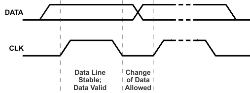
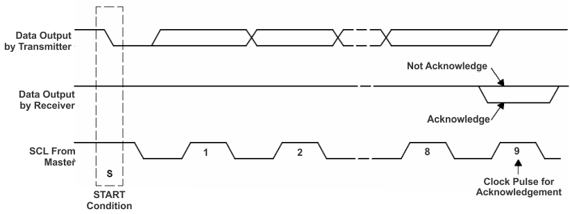
The master then generates the SCL pulses, and transmits the address and the read/write direction bit R/W on the SDA line. During all transmissions, the master ensures that data is valid. A valid data condition requires the SDA line to be stable during the entire high period of the clock pulse (see Figure 9-8). All devices recognize the address sent by the master and compare it to their internal fixed addresses. Only the slave device with a matching address generates and acknowledge (see Figure 9-9) by pulling the SDA line low during the entire high period of the ninth SCL cycle. Upon detecting the acknowledge, the master knows that communication link with a slave has been established.
 Figure 9-8 Bit Transfer on the Serial Interface
 Figure 9-9 Acknowledge on the I2C Bus
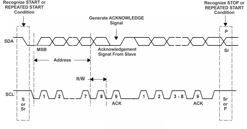
The master generates further SCL cycles to either transmit data to the slave (R/W bit 0) or receive data from the slave (R/W bit 1). In either case, the receiver needs to acknowledge the data sent by the transmitter. An acknowledge signal can either be generated by the master or by the slave, depending on which on is the receiver. The 9-bit valid data sequences consisting of 8-bit data and 1-bit acknowledge can continue as long as necessary. To signal the end of the data transfer, the master generates a stop condition by pulling the SDA line from low to high while the SCL line is high (see Figure 9-10). This releases the bus and stops the communication link with the addressed slave. All I2C compatible devices must recognize the STOP condition. Upon the receipt of a STOP condition, all devices know that the bus is released, and wait for a START condition followed by a matching address. If a transaction is terminated prematurely, the master needs to send a STOP condition to prevent the slave I2C logic from remaining in an incorrect state. Attempting to read data from register addresses not listed in this section results in 0xFFh being read out.
 Figure 9-10 Bus Protocol