ZHCSJZ9B june   2019  – august 2023 BQ25155

PRODUCTION DATA  

  1.   1
  2. 特性
  3. 应用
  4. 说明
  5. Revision History
  6. 说明(续)
  7. Device Key Default Settings
  8. Pin Configuration and Functions
  9. Specifications
    1. 8.1 Absolute Maximum Ratings
    2. 8.2 ESD Ratings
    3. 8.3 Recommended Operating Conditions
    4. 8.4 Thermal Information
    5. 8.5 Electrical Characteristics
    6. 8.6 Timing Requirements
    7. 8.7 Typical Characteristics
  10. Detailed Description
    1. 9.1 Overview
    2. 9.2 Functional Block Diagram
    3. 9.3 Feature Description
      1. 9.3.1  Linear Charger and Power Path
        1. 9.3.1.1 Battery Charging Process
          1. 9.3.1.1.1 Pre-Charge
          2. 9.3.1.1.2 Fast Charge
          3. 9.3.1.1.3 Pre-Charge to Fast Charge Transitions and Charge Current Ramping
          4. 9.3.1.1.4 Termination
        2. 9.3.1.2 JEITA and Battery Temperature Dependent Charging
        3. 9.3.1.3 Input Voltage Based Dynamic Power Management (VINDPM) and Dynamic Power Path Management (DPPM)
        4. 9.3.1.4 Battery Supplement Mode
      2. 9.3.2  Protection Mechanisms
        1. 9.3.2.1 Input Over-Voltage Protection
        2. 9.3.2.2 Safety Timer and I2C Watchdog Timer
        3. 9.3.2.3 Thermal Protection and Thermal Charge Current Foldback
        4. 9.3.2.4 Battery Short and Over Current Protection
        5. 9.3.2.5 PMID Short Circuit
      3. 9.3.3  ADC
        1. 9.3.3.1 ADC Operation in Active Battery Mode and Low Power Mode
        2. 9.3.3.2 ADC Operation When VIN Present
        3. 9.3.3.3 ADC Measurements
        4. 9.3.3.4 ADC Programmable Comparators
      4. 9.3.4  VDD LDO
      5. 9.3.5  Load Switch/LDO Output and Control
      6. 9.3.6  PMID Power Control
      7. 9.3.7  System Voltage (PMID) Regulation
      8. 9.3.8  MR Wake and Reset Input
        1. 9.3.8.1 MR Wake or Short Button Press Functions
        2. 9.3.8.2 MR Reset or Long Button Press Functions
      9. 9.3.9  14-Second Watchdog for HW Reset
      10. 9.3.10 Faults Conditions and Interrupts ( INT)
        1. 9.3.10.1 Flags and Fault Condition Response
      11. 9.3.11 Power Good ( PG) Pin
      12. 9.3.12 External NTC Monitoring (TS)
        1. 9.3.12.1 TS Thresholds
      13. 9.3.13 External NTC Monitoring (ADCIN)
      14. 9.3.14 I2C Interface
        1. 9.3.14.1 F/S Mode Protocol
    4. 9.4 Device Functional Modes
      1. 9.4.1 Ship Mode
      2. 9.4.2 Low Power
      3. 9.4.3 Active Battery
      4. 9.4.4 Charger/Adapter Mode
      5. 9.4.5 Power-Up/Down Sequencing
    5. 9.5 Register Map
      1. 9.5.1 I2C Registers
  11. 10Application and Implementation
    1. 10.1 Application Information
    2. 10.2 Typical Application
      1. 10.2.1 Design Requirements
      2. 10.2.2 Detailed Design Procedure
        1. 10.2.2.1 Input (IN/PMID) Capacitors
        2. 10.2.2.2 VDD, LDO Input and Output Capacitors
        3. 10.2.2.3 TS
        4. 10.2.2.4 Recommended Passive Components
      3. 10.2.3 Application Curves
  12. 11Power Supply Recommendations
  13. 12Layout
    1. 12.1 Layout Guidelines
    2. 12.2 Layout Example
  14. 13Device and Documentation Support
    1. 13.1 Device Support
      1. 13.1.1 第三方米6体育平台手机版_好二三四免责声明
    2. 13.2 Documentation Support
      1. 13.2.1 Related Documentation
    3. 13.3 接收文档更新通知
    4. 13.4 支持资源
    5. 13.5 静电放电警告
    6. 13.6 Trademarks
    7. 13.7 术语表
  15. 14Mechanical, Packaging, and Orderable Information

封装选项

机械数据 (封装 | 引脚)
散热焊盘机械数据 (封装 | 引脚)
订购信息

Ship Mode

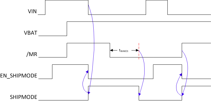
Ship Mode is the lowest quiescent current state for the device. Ship Mode latches off the device and BAT FET until VIN > VUVLO or the MR button is depressed for tWAKE1 and released. Ship mode can be entered regardless of the state of CE. The device will also enter Ship Mode upon battery insertion when no valid VIN is present. If the EN_SHIPMODE is written to a 1 while a valid input supply is connected, the device will wait until the IN supply is removed to enter ship mode. If the MR pin is held low when the EN_SHIPMODE bit is set, the device will wait until the MR pin goes high before entering Ship Mode. Figure 9-13 shows this behavior. The battery voltage must be above the maximum programmable VBATUVLO threshold in order to exit Ship Mode with MR press. The EN_SHIPMODE bit can be cleared using the I2C interface while the VIN input is valid. The EN_SHIPMODE bit is not cleared upon the I2C watchdog expiring, this means that if watchdog timer fault occurs while the EN_SHIPMODE bit is set and the device is waiting to go into Ship Mode because VIN is present or MR is low, the device will still proceed to go into Ship Mode once those conditions are cleared. The following list shows the functions that are active during Ship Mode:

  • VIN_UVLO Comparator
  • MR Input

GUID-8663157C-B14C-484D-BE2B-1F435FFFF369-low.gif Figure 9-13 Ship Mode Entry Based On EN_SHIPMODE bit