ZHCSLW6A december   2020  – august 2023 BQ25157

PRODUCTION DATA  

  1.   1
  2. 特性
  3. 应用
  4. 说明
  5. Revision History
  6. 说明(续)
  7. Device Key Default Settings
  8. Pin Configuration and Functions
  9. Specifications
    1. 8.1 Absolute Maximum Ratings
    2. 8.2 ESD Ratings
    3. 8.3 Recommended Operating Conditions
    4. 8.4 Thermal Information
    5. 8.5 Electrical Characteristics
    6. 8.6 Timing Requirements
    7. 8.7 Typical Characteristics
  10. Detailed Description
    1. 9.1 Overview
    2. 9.2 Functional Block Diagram
    3. 9.3 Feature Description
      1. 9.3.1  Linear Charger and Power Path
        1. 9.3.1.1 Battery Charging Process
          1. 9.3.1.1.1 Pre-Charge
          2. 9.3.1.1.2 Fast Charge
          3. 9.3.1.1.3 Pre-Charge to Fast Charge Transitions and Charge Current Ramping
          4. 9.3.1.1.4 Termination
        2. 9.3.1.2 JEITA and Battery Temperature Dependent Charging
        3. 9.3.1.3 Input Voltage Based Dynamic Power Management (VINDPM) and Dynamic Power Path Management (DPPM)
        4. 9.3.1.4 Battery Supplement Mode
      2. 9.3.2  Protection Mechanisms
        1. 9.3.2.1 Input Over-Voltage Protection
        2. 9.3.2.2 Safety Timer and I2C Watchdog Timer
        3. 9.3.2.3 Thermal Protection and Thermal Charge Current Foldback
        4. 9.3.2.4 Battery Short and Over Current Protection
        5. 9.3.2.5 PMID Short Circuit
      3. 9.3.3  ADC
        1. 9.3.3.1 ADC Operation in Active Battery Mode and Low Power Mode
        2. 9.3.3.2 ADC Operation When VIN Present
        3. 9.3.3.3 ADC Measurements
        4. 9.3.3.4 ADC Programmable Comparators
      4. 9.3.4  VDD LDO
      5. 9.3.5  Load Switch/LDO Output and Control
      6. 9.3.6  PMID Power Control
      7. 9.3.7  MR Wake and Reset Input
        1. 9.3.7.1 MR Wake or Short Button Press Functions
        2. 9.3.7.2 MR Reset or Long Button Press Functions
      8. 9.3.8  14-Second Watchdog for HW Reset
      9. 9.3.9  Faults Conditions and Interrupts ( INT)
        1. 9.3.9.1 Flags and Fault Condition Response
      10. 9.3.10 Power Good ( PG) Pin
      11. 9.3.11 External NTC Monitoring (TS)
        1. 9.3.11.1 TS Thresholds
      12. 9.3.12 External NTC Monitoring (ADCIN)
      13. 9.3.13 I2C Interface
        1. 9.3.13.1 F/S Mode Protocol
    4. 9.4 Device Functional Modes
      1. 9.4.1 Ship Mode
      2. 9.4.2 Low Power
      3. 9.4.3 Active Battery
      4. 9.4.4 Charger/Adapter Mode
      5. 9.4.5 Power-Up/Down Sequencing
    5. 9.5 Register Map
      1. 9.5.1 I2C Registers
  11. 10Application and Implementation
    1. 10.1 Application Information
    2. 10.2 Typical Application
      1. 10.2.1 Design Requirements
      2. 10.2.2 Detailed Design Procedure
        1. 10.2.2.1 Input (IN/PMID) Capacitors
        2. 10.2.2.2 VDD, LDO Input and Output Capacitors
        3. 10.2.2.3 TS
        4. 10.2.2.4 Recommended Passive Components
      3. 10.2.3 Application Curves
  12. 11Power Supply Recommendations
  13. 12Layout
    1. 12.1 Layout Guidelines
    2. 12.2 Layout Example
  14. 13Device and Documentation Support
    1. 13.1 Device Support
      1. 13.1.1 第三方米6体育平台手机版_好二三四免责声明
    2. 13.2 Documentation Support
      1. 13.2.1 Related Documentation
    3. 13.3 接收文档更新通知
    4. 13.4 支持资源
    5. 13.5 静电放电警告
    6. 13.6 Trademarks
    7. 13.7 术语表
  15. 14Mechanical, Packaging, and Orderable Information

封装选项

机械数据 (封装 | 引脚)
散热焊盘机械数据 (封装 | 引脚)
订购信息

TS Thresholds

The BQ25157 monitors the TS voltage and sends an interrupt to the host whenever it crosses the VHOT, VWARM, VCOOL and VCOLD thresholds which correspond to different temperature thresholds based on the NTC resistance and biasing. These thresholds may be adjusted through I2C by the host. The device will also disable charging if TS pin exceeds the VTS_OPEN threshold.

The TS biasing circuit is shown in Figure 9-8. The ADC range is set to 1.2 V. Note that the respective VTSand hence ADC reading for TCOLD (0°C), TCOOL (10°C), TWARM (45°C) and THOT (60°C) changes for every NTC, therefore the threshold values may need to be adjusted through I2C based on the supported NTC type.
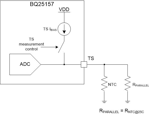
GUID-20200930-CA0I-78NX-RKS0-R8Z3WN1K0SMM-low.gif Figure 9-8 TS Bias Functional Diagram

The BQ25157 supports by default the following thresholds for a 10-KΩ NTC.

Table 9-6 TS Thresholds for 10-KΩ Thermistor
THRESHOLDTEMPERATURE
(°C)
VTS (V)
Open-->0.9
Cold00.585
Cool100.514
Warm450.265
Hot600.185

For accurate temperature thresholds a 10-KΩ NTC with a 3380 B-constant should be used (Murata NCP03XH103F05RL for example) with a parallel 10-KΩ resistor. Each threshold can be programmed via I2C through the TS_COLD, TS_COOL, TS_WARM and TS_HOT registers. The value in the registers corresponds to the 8 MSBs in the TS ADC output code.