ZHCSNP0A august 2020 – march 2021 BQ25171-Q1
PRODUCTION DATA
- 1
- 1 特性
- 2 应用
- 3 说明
- 4 Revision History
- 5 Pin Configuration and Functions
- 6 Specifications
- 7 Detailed Description
- 8 Application and Implementation
- 9 Power Supply Recommendations
- 10Layout
- 11Device and Documentation Support
- 12Mechanical, Packaging, and Orderable Information
请参考 PDF 数据表获取器件具体的封装图。
机械数据 (封装 | 引脚)
- DRC|10
散热焊盘机械数据 (封装 | 引脚)
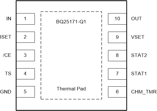
5 Pin Configuration and Functions
 Figure 5-1 VSON
Package10-Pin(Top
View)
Figure 5-1 VSON
Package10-Pin(Top
View)Table 5-1 Pin Functions
| PIN | I/O | DESCRIPTION | |
|---|---|---|---|
| NAME | NUMBER | ||
| IN | 1 | P | Input power, connected to external DC supply. Bypass IN with at least 1-μF capacitor to GND, placed close to the IC. |
| ISET | 2 | I | Programs the fast-charge current setting. External resistor from ISET to GND defines fast-charge current value. Recommended range is 30 kΩ (10 mA) to 375 Ω (800 mA). ICHG = KISET / RISET. Precharge current is defined as 20% of ICHG. Termination current is defined as 10% of ICHG. |
| CE | 3 | I | Active Low Charge Enable pin. Battery charging is enabled when CE pin is low. IC remains in Shutdown Mode and battery charging is disabled when CE pin is high. An internal pulldown resistor (RPD_CE) enables the IC by default if this pin is floating. |
| TS | 4 | I | Temperature Qualification Voltage Input. Connect a negative temperature coefficient (NTC) thermistor directly from TS to GND (AT103-2 recommended). Charge suspends when the TS pin voltage is out of range. If TS function is not needed, connect an external 10-kΩ resistor from TS to GND. |
| GND | 5 | – | Ground pin |
| CHM_TMR | 6 | I | Programs the chemistry and charge time to be used with a pulldown resistor. Valid resistor range is 3.6 kΩ to 100 kΩ, values outside this range will suspend charge. Refer to Section 7.3.1.2 for voltage level details. |
| STAT1 | 7 | O | Open drain charge status 1 output. Connect to pullup rail via 10-kΩ resistor. |
| STAT2 | 8 | O | Open drain charge status 2 output. Connect to pullup rail via 10-kΩ resistor. |
| VSET | 9 | I | Programs the regulation voltage for OUT pin with a pull-down resistor. Valid resistor range is 3.6 kΩ to 100 kΩ, values outside this range will suspend charge. Refer to Section 7.3.1.3 for voltage level details. |
| OUT | 10 | P | Battery Connection. System load may be connected in parallel to battery. Bypass OUT with at least 1-μF capacitor to GND, placed close to the IC. |
| Thermal Pad | — | — | Exposed pad beneath the IC for heat dissipation. Solder thermal pad to the board with vias connecting to solid GND plane. |