ZHCSQ82 September 2022 BQ25176M
PRODUCTION DATA
- 1 特性
- 2 应用
- 3 说明
- 4 Revision History
- 5 Pin Configuration and Functions
- 6 Specifications
- 7 Detailed Description
- 8 Application and Implementation
- 9 Power Supply Recommendations
- 10Layout
- 11Device and Documentation Support
- 12Mechanical, Packaging, and Orderable Information
5 Pin Configuration and Functions
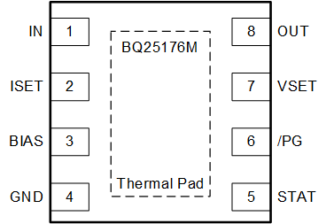
 Figure 5-1 DSG Package8-Pin WSONTop
View
Figure 5-1 DSG Package8-Pin WSONTop
ViewTable 5-1 Pin Functions
| PIN | I/O | DESCRIPTION | |
|---|---|---|---|
| NAME | NUMBER | ||
| IN | 1 | P | Input power, connected to external DC supply. Bypass IN with at least 1-μF capacitor to GND, placed close to the IC. |
| ISET | 2 | I | Programs the device fast-charge current. External resistor from ISET to GND defines fast charge current value. Expected range is 30 kΩ (10 mA) to 375 Ω (800 mA). ICHG = KISET / RISET. Precharge current is defined as 20% of ICHG. Termination current is defined as 10% of ICHG. |
BIAS | 3 | I | Bias sense pin. Connect an external 10-kΩ resistor from this pin to GND. This pin can also be used as a charging disable pin by pulling the pin to GND by means of an external NMOS. Refer to the applications section for more information. |
| GND | 4 | – | Ground pin |
| STAT | 5 | O | Open drain charger status indication output. Connect to pull-up rail via 10-kΩ resistor. LOW indicates charge in progress. HIGH indicates charge complete or charge disabled. When a fault condition is detected STAT pin blinks at 1 Hz. |
| PG | 6 | O | Open drain charge power good indication output. Connect to pull-up rail via 10-kΩ resistor. PG pulls low when VIN > VIN_LOWV and VOUT + VSLEEPZ < VIN < VIN_OV. |
| VSET | 7 | I | Programs the regulation voltage for OUT pin with a pull-down resistor. Valid resistor range is 18.2 kΩ to 100 kΩ, values outside this range will suspend charge. Refer to Section 7.3.1.2 for voltage level details. Recommend using ±1% tolerance resistor with <200 ppm/ºC temperature coefficient. |
| OUT | 8 | P | Battery connection. System Load may be connected in parallel to battery. Bypass OUT with at least 1-μF capacitor to GND, placed close to the IC. |
| Thermal Pad | — | — | Exposed pad beneath the IC for heat dissipation. Solder thermal pad to the board with vias connecting to solid GND plane. |