ZHCSPC2C September 2021 – January 2023 BQ25180
PRODUCTION DATA
- 1 特性
- 2 应用
- 3 说明
- 4 Revision History
- 5 说明(续)
- 6 Pin Configuration and Functions
- 7 Specifications
-
8 Detailed Description
- 8.1 Overview
- 8.2 Functional Block Diagram
- 8.3
Feature Description
- 8.3.1 Input Voltage Based Dynamic Power Management (VINDPM)
- 8.3.2 Dynamic Power Path Management Mode (DPPM)
- 8.3.3 Battery Supplement Mode
- 8.3.4 SYS Power Control (SYS_MODE bit control)
- 8.3.5 SYS Regulation
- 8.3.6 ILIM Control
- 8.3.7 Protection Mechanisms
- 8.3.8 Pushbutton Wake and Reset Input
- 8.3.9 15-Second Timeout for HW Reset
- 8.3.10 Hardware Reset
- 8.3.11 Software Reset
- 8.3.12 Interrupt Indicator (/INT) Pin
- 8.3.13 External NTC Monitoring (TS)
- 8.3.14 I2C Interface
- 8.4 Device Functional Modes
- 8.5 Register Maps
- 9 Application and Implementation
- 10Power Supply Recommendations
- 11Layout
- 12Device and Documentation Support
- 13Mechanical, Packaging, and Orderable Information
8.3.14.1 F/S Mode Protocol
The master initiates a data transfer by generating a start condition. The start condition is when a high-to-low transition occurs on the SDA line while SCL is high, as shown in Figure 8-6. All I2C-compatible devices should recognize a start condition.
 Figure 8-6 START and STOP Condition
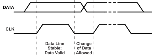
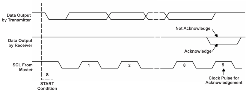
The master then generates the SCL pulses, and transmits the 8-bit address and the read/write direction bit R/W on the SDA line. During all transmissions, the master ensures that data is valid. A valid data condition requires the SDA line to be stable during the entire high period of the clock pulse (see Figure 8-7). All devices recognize the address sent by the master and compare it to their internal fixed addresses. Only the slave device with a matching address generates an acknowledge (see Figure 8-8) by pulling the SDA line low during the entire high period of the ninth SCL cycle. Upon detecting this acknowledge, the master knows that communication link with a slave has been established.
 Figure 8-7 Bit Transfer on the Serial
Interface
Figure 8-7 Bit Transfer on the Serial
InterfaceThe master generates further SCL cycles to either transmit data to the slave (R/W bit 1) or receive data from the slave (R/W bit 0). In either case, the receiver needs to acknowledge the data sent by the transmitter. So an acknowledge signal can either be generated by the master or by the slave, depending on which one is the receiver. The 9-bit valid data sequences consisting of 8-bit data and 1-bit acknowledge can continue as long as necessary. To signal the end of the data transfer, the master generates a stop condition by pulling the SDA line from low to high while the SCL line is high (see Figure 8-6). This releases the bus and stops the communication link with the addressed slave. All I2C compatible devices must recognize the stop condition. Upon the receipt of a stop condition, all devices know that the bus is released, and wait for a start condition followed by a matching address. If a transaction is terminated prematurely, the master needs to send a STOP condition to prevent the slave I2C logic from remaining in an incorrect state. Attempting to read data from register addresses not listed in this section will result in FFh being read out.
 Figure 8-8 Ackowledge on the I2C
Bus
 Figure 8-9 Bus Protocol