ZHCSMH4A march 2020 – november 2020 BQ25306
PRODUCTION DATA
- 1
- 1 特性
- 2 应用
- 3 说明
- 4 Revision History
- 5 说明(续)
- 6 Device Comparison Table
- 7 Pin Configuration and Functions
- 8 Specifications
-
9 Detailed Description
- 9.1 Overview
- 9.2 Functional Block Diagram
- 9.3 Feature Description
- 9.4 Device Functional Modes
- 10Application and Implementation
- 11Power Supply Recommendations
- 12Layout
- 13Device and Documentation Support
- 14Mechanical, Packaging, and Orderable Information
7 Pin Configuration and Functions
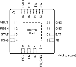
 Figure 7-1 RTE Package16-Pin WQFNTop View
Table 7-1 Pin Functions
| PIN | I/O(1) | DESCRIPTION | |
|---|---|---|---|
| NAME | NO. | ||
| VBUS | 1 | P | Charger input voltage. The internal n-channel reverse block MOSFET (RBFET) is connected between VBUS and PMID with VBUS on source. Place a 2.2uF ceramic capacitor from VBUS to GND and place it as close as possible to IC. |
| PMID | 16 | P | Connected to the drain of the reverse blocking MOSFET (RBFET) and the drain of high-side MOSFET (HSFET). Place ceramic 10μF on PMID to GND and place it as close as possible to IC. |
| SW | 13,14 | P | Switching node. Connected to output inductor. Internally SW is connected to the source of the n-channel HSFET and the drain of the n-channel LSFET. Connect the 0.047μF bootstrap capacitor from SW to BTST. |
| BTST | 15 | P | High-side FET driver supply. Internally, the BTST is connected to the cathode of the internal boost-strap diode. Connect the 0.047μF bootstrap capacitor from SW to BTST. |
| GND | 11,12 | P | Ground. Connected directly to thermal pad on the top layer. A single point connection is recommended between power ground and analog ground near the IC GND pins. |
| REGN | 2 | P | Low-side FET driver positive supply output. Connect a 2.2μF ceramic capacitor from REGN to GND. The capacitor should be placed close to the IC. |
| BAT | 10 | AI | Battery voltage sensing input. Connect this pin to the positive terminal of the battery pack and the node of inductor output terminal. 10-µF capacitor is recommended to connect to this pin. |
| TS | 7 | AI | Battery temperature voltage input. Connect a negative temperature coefficient thermistor (NTC). Program temperature window with a resistor divider from REGN to TS and TS to GND. Charge suspends when TS pin voltage is out of range. When TS pin is not used, connect a 10-kΩ resistor from REGN to TS and a 10-kΩ resistor from TS to GND. It is recommended to use a 103AT-2 thermistor. |
| ICHG | 4 | AI | Charge current program input. Connect a 1% resistor RICHG from this pin to ground to program the charge current as ICHG = KICHG / RICHG (KICHG = 40,000). No capacitor is allowed to connect at this pin. When ICHG pin is pulled to ground or left open, the charger stop switching and STAT pin starts blinking. |
| STAT | 3 | AO | Charge status indication output. This pin is open drain output.
Connect this pin to REGN via a current limiting resistor and LED.
The STAT pin indicates charger status as:
|
| FB | 9 | AI | Battery voltage feedback input. Connect this pin to resistor divider’s middle point to program battery charge voltage. When this pin is shorted to GND or open by fault, the converter stop switching and STAT pin blinks. The resistor divider consists of a resistor R1 from battery positive terminal to FB pin and a resistor R2 from FB pin to FB_GND. The recommended resistance value of R2 is 200kΩ or lower. The battery charge voltage is programmed as VBATREG = 1.1 (1 + R1/R2). The voltage regulation loop is internally compensated and a 470pF feedforward capacitor is recommended to connect from battery to FB pin. |
| FB_GND | 8 | AI | Battery voltage feedback ground input. Connect the feedback resistor divider's low side resister to this pin. The input of this pin is in high impedance when adaptor is unplugged or the charger is disabled by EN pin. |
| POL | 5 | AI | EN pin polority selection. Keep this pin floating for standalone charger. |
| EN | 6 | AI | Device sisable input. With POL pin floating, the device is enabled with EN pin floating or pulled low, and the device is disabled if EN pin is pulled high. With POL pin grounded, the device is enabled with EN pin pulled high, and the device is disabled with EN pin pulled low or floating. |
| Thermal Pad | 17 | - | Ground reference for the device that is also the thermal pad used to conduct heat from the device. This connection serves two purposes. The first purpose is to provide an electrical ground connection for the device. The second purpose is to provide a low thermal-impedance path from the device die to the PCB. This pad should be tied externally to a ground plane. Ground layer(s) are connected to thermal pad through vias under thermal pad. |
(1) AI = Analog input, AO = Analog Output, AIO = Analog input
Output, DI = Digital input, DO = Digital Output, DIO = Digital input Output, P =
Power